⬇ Download Markdown · ⬇ Download LaTeX · ⬇ original · view original · CSV: table 1, table 2, table 3, table 4, table 5, table 6, table 7, table 8, table 9, table 10, table 11, table 12, table 13, table 14, table 15, table 16, table 17, table 18, table 19, table 20, table 21, table 22, table 23, table 24, table 25, table 26, table 27, table 28, table 29, table 30, table 31, table 32, table 33, table 34
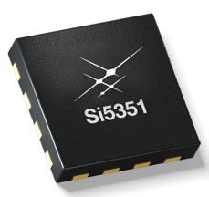
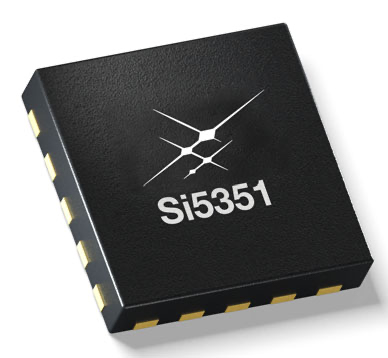
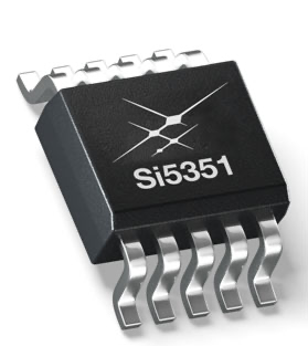
https://www.skyworksinc.com/Products/Timi Glitchless frequency changes ng/CMOS-Clock-Generators Separate voltage supply pins Generates up to eight non-integerrelated frequencies from 2.5 kHz to 200 MHz I 2 C user definable configuration Exact frequency synthesis at each output (0 ppm error) Highly linear VCXO Optional clock input (CLKIN) Low output period jitter: < 70 ps pp, typ Configurable spread spectrum selectable at each output Operates from a low-cost, fixed frequency crystal: 25 or 27 MHz Supports static phase offset Programmable rise/fall time control provide level translation: Core VDD: 2.5 or 3.3 V Output VDDO: 1.8, 2.5, or 3.3 V Excellent PSRR eliminates external power supply filtering Very low power consumption Adjustable output delay Available in three packages types: 10-MSOP: 3 outputs 16-QFN (3x3 mm): 4 outputs 20-QFN (4x4 mm): 8 outputs PCIE Gen 1 compatible Supports HCSL compatible swing 10-MSOP 16-QFN 20-QFN
Audio/video equipment, gaming Printers, scanners, projectors Handheld Instrumentation Laser range finder Residential gateways Networking/communication Servers, storage XO replacement
Ordering Information:
See page 34
The Si5351 is an I 2 C configurable clock generator that is ideally suited for replacing crystals, crystal oscillators, VCXOs, phase-locked loops (PLLs), and fanout buffers in cost-sensitive applications. Based on a PLL/VCXO + high resolution MultiSynth fractional divider architecture, the Si5351 can generate any frequency up to 200 MHz on each of its outputs with 0 ppm error. Three versions of the Si5351 are available to meet a wide variety of applications. The Si5351A generates up to 8 free-running clocks using an internal oscillator for replacing crystals and crystal oscillators. The Si5351B adds an internal VCXO and provides the flexibility to replace both free-running clocks and synchronous clocks. It eliminates the need for higher cost, custom pullable crystals while providing reliable operation over a wide tuning range. The Si5351C offers the same flexibility but synchronizes to an external reference clock (CLKIN).
Skyworks Solutions, Inc. • Phone [781] 376-3000 • Fax [781] 376-3100 • [email protected] • www.skyworksinc.com Rev. 1.3 • Skyworks Proprietary Information • Products and Product Information are Subject to Change Without Notice • August 27, 2021
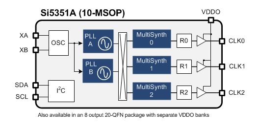
| XA | OSC | PLL A | MultiSynth 0 | R0 | VDDOACLK0 |
|---|---|---|---|---|---|
| XB | MultiSynth 1 | R1 | CLK1 | ||
| PLL B | MultiSynth 2 | R2 | VDDOBCLK2 | ||
| MultiSynth 3 | R3 | CLK3 | |||
| A0 SDA | I2 C | MultiSynth 4 | R4 | VDDOCCLK4 | |
| SCL | MultiSynth 5 | R5 | CLK5 | ||
| OEB | Control | MultiSynth 6 | R6 | VDDODCLK6 | |
| SSEN | Logic | MultiSynth 7 | R7 | CLK7 |
VDDOB CLK2 CLK3
VDDOC CLK4 CLK5
VDDOD CLK6 CLK7
| XA | OSC | PLL A | MultiSynth 0 | R0 | VDDOACLK0 |
|---|---|---|---|---|---|
| XB | MultiSynth | VDDOB | |||
| PLL | 1 | R1 | CLK1 | ||
| A0 SDA | I2 C | B | MultiSynth 2 | R2 | VDDOCCLK2 |
| SCL | MultiSynth 3 | R3 | VDDODCLK3 | ||
| OEB | Control Logic | ||||
| 1 | R1 | CLK1 | |||
| VC | vcxo | MultiSynth | VDDOC | ||
| SDA SCL | I2 C | 2 MultiSynth 3 | R2 R3 | CLK2VDDODCLK3 | |
| OEB | Control Logic |
4 R4 MultiSynth
5 R5 MultiSynth
6 R6 MultiSynth
7 R7 VDDOA CLK0 CLK1
VDDOB CLK2 CLK3
VDDOC CLK4 CLK5
VDDOD CLK6 CLK7 Skyworks Solutions, Inc. • Phone [781] 376-3000 • Fax [781] 376-3100 • [email protected] • www.skyworksinc.com Rev. 1.3 • Skyworks Proprietary Information • Products and Product Information are Subject to Change Without Notice • August 27, 2021
Si5351C (20-QFN)
XA
OSC XB PLL A PLL B CLKIN SDA SCL I 2 C INTR OEB Control Logic MultiSynth
0 R0 MultiSynth
1 R1 MultiSynth
2 R2 MultiSynth
3 R3 MultiSynth
4 R4 MultiSynth
5 R5 MultiSynth
6 R6 MultiSynth
7 R7 VDDOA CLK0 CLK1
VDDOB CLK2 CLK3
VDDOC CLK4 CLK5
VDDOD CLK6 CLK7
XA
| MultiSynth | VDDOA | ||||
|---|---|---|---|---|---|
| XAXB | OSC | PLL A | 0 MultiSynth 1 | R0 R1 | CLK0CLK1 |
| MultiSynth | VDDOB | ||||
| CLKIN | PLL B | 2 | R2 | CLK2 | |
| MultiSynth 3 | R3 | CLK3 | |||
| SDA | MultiSynth 4 | R4 | VDDOCCLK4 | ||
| SCL INTR | I2 C | MultiSynth 5 MultiSynth | R5 | CLK5VDDOD | |
| 6 | R6 | CLK6 | |||
| OEB | Control Logic | MultiSynth 7 | R7 | CLK7 | |
XA
OSC XB PLL A vcxo VC SDA SCL I C
OEB Control Logic 2 Si5351C (16-QFN)
XA
OSC XB PLL A PLL B CLKIN SDA SCL I C
OEB Control Logic 2 MultiSynth
0 R0 VDDOA CLK0
MultiSynth
1 R1 VDDOB CLK1
MultiSynth
2 R2 VDDOC CLK2
MultiSynth
3 R3 VDDOD CLK3 Skyworks Solutions, Inc. • Phone [781] 376-3000 • Fax [781] 376-3100 • [email protected] • www.skyworksinc.com 3 Rev. 1.3 • Skyworks Proprietary Information • Products and Product Information are Subject to Change Without Notice • August 27, 2021
| Part Number | I2 C or Pin | Frequency Reference | Programmed? | Outputs | Datasheet |
|---|---|---|---|---|---|
| Si5351A-B-GT | I2 C | XTAL only | Blank | 3 | Si5351A/B/C-B |
| Si5351A-B-GM1 | I2 C | XTAL only | Blank | 4 | Si5351A/B/C-B |
| Si5351B-B-GM1 | I2 C | XTAL and/or Voltage | Blank | 4 | Si5351A/B/C-B |
| Si5351C-B-GM1 | I2 C | XTAL and/or CLKIN | Blank | 4 | Si5351A/B/C-B |
| Si5351A-B-GM | I2 C | XTAL only | Blank | 8 | Si5351A/B/C-B |
| Si5351B-B-GM | I2 C | XTAL and/or Voltage | Blank | 8 | Si5351A/B/C-B |
| Si5351C-B-GM | I2 C | XTAL and/or CLKIN | Blank | 8 | Si5351A/B/C-B |
| Si5351A-Bxxxxx-GT | I2 C | XTAL only | Factory Preprogrammed | 3 | Si5351A/B/C-B |
| Si5351A-Bxxxxx-GM1 | I2 C | XTAL only | Factory Preprogrammed | 4 | Si5351A/B/C-B |
| Si5351B-Bxxxxx-GM1 | I2 C | XTAL and/or Voltage | Factory Preprogrammed | 4 | Si5351A/B/C-B |
| Si5351C-Bxxxxx-GM1 | I2 C | XTAL and/or CLKIN | Factory Preprogrammed | 4 | Si5351A/B/C-B |
| Si5351A-Bxxxxx-GM | I2 C | XTAL only | Factory Preprogrammed | 8 | Si5351A/B/C-B |
| Si5351B-Bxxxxx-GM | I2 C | XTAL and/or Voltage | Factory Preprogrammed | 8 | Si5351A/B/C-B |
| Si5351C-Bxxxxx-GM | I2 C | XTAL and/or CLKIN | Factory Preprogrammed | 8 | Si5351A/B/C-B |
| Si5350A-Bxxxxx-GT | Pin | XTAL only | Factory Preprogrammed | 3 | Si5350A-B |
| Si5350A-Bxxxxx-GM1 | Pin | XTAL only | Factory Preprogrammed | 4 | Si5350A-B |
| Si5350A-Bxxxxx-GM | Pin | XTAL only | Factory Preprogrammed | 8 | Si5350A-B |
| Si5350B-Bxxxxx-GT | Pin | XTAL and/or Voltage | Factory Preprogrammed | 3 | Si5350B-B |
| Si5350B-Bxxxxx-GM1 | Pin | XTAL and/or Voltage | Factory Preprogrammed | 4 | Si5350B-B |
| Si5350B-Bxxxxx-GM | Pin | XTAL and/or Voltage | Factory Preprogrammed | 8 | Si5350B-B |
| Si5350C-Bxxxxx-GT | Pin | XTAL and/or CLKIN | Factory Preprogrammed | 3 | Si5350C-B |
| Si5350C-Bxxxxx-GM1 | Pin | XTAL and/or CLKIN | Factory Preprogrammed | 4 | Si5350C-B |
| Si5350C-Bxxxxx-GM | Pin | XTAL and/or CLKIN | Factory Preprogrammed | 8 | Si5350C-B |
| Notes: 1. XTAL = 25/27 MHz, Voltage = 0 to VDD, CLKIN = 10 to 100 MHz. "xxxxx" = unique custom code. 2. Create custom, factory preprogrammed parts using ClockBuilder Pro. | Notes: 1. XTAL = 25/27 MHz, Voltage = 0 to VDD, CLKIN = 10 to 100 MHz. "xxxxx" = unique custom code. 2. Create custom, factory preprogrammed parts using ClockBuilder Pro. | Notes: 1. XTAL = 25/27 MHz, Voltage = 0 to VDD, CLKIN = 10 to 100 MHz. "xxxxx" = unique custom code. 2. Create custom, factory preprogrammed parts using ClockBuilder Pro. | Notes: 1. XTAL = 25/27 MHz, Voltage = 0 to VDD, CLKIN = 10 to 100 MHz. "xxxxx" = unique custom code. 2. Create custom, factory preprogrammed parts using ClockBuilder Pro. | Notes: 1. XTAL = 25/27 MHz, Voltage = 0 to VDD, CLKIN = 10 to 100 MHz. "xxxxx" = unique custom code. 2. Create custom, factory preprogrammed parts using ClockBuilder Pro. | Notes: 1. XTAL = 25/27 MHz, Voltage = 0 to VDD, CLKIN = 10 to 100 MHz. "xxxxx" = unique custom code. 2. Create custom, factory preprogrammed parts using ClockBuilder Pro. |
4 Skyworks Solutions, Inc. • Phone [781] 376-3000 • Fax [781] 376-3100 • [email protected] • www.skyworksinc.com
Rev. 1.3 • Skyworks Proprietary Information • Products and Product Information are Subject to Change Without Notice • August 27, 2021
Resource
Si5350/51 Frequently Asked Questions ClockBuilder Pro (CBPro) Software Si535x Development Kits URL
https://www.skyworksinc.com/en/Products/Timing
https://www.skyworksinc.com/en/Application-Pages/ClockbuilderPro-Software
https://www.skyworksinc.com/en/Products/Timing/EvaluationKits/si535x-b20qfn-evb-evaluation-kit Skyworks Solutions, Inc. • Phone [781] 376-3000 • Fax [781] 376-3100 • [email protected] • www.skyworksinc.com 5 Rev. 1.3 • Skyworks Proprietary Information • Products and Product Information are Subject to Change Without Notice • August 27, 2021
4.1. Input Stage . . . . . . . . . . . . . . . . . . . . . . . . . . . . . . . . . . . . . . . . . . . . . . . . . . . . . . . . 15 4.2. Synthesis Stages . . . . . . . . . . . . . . . . . . . . . . . . . . . . . . . . . . . . . . . . . . . . . . . . . . . 16 4.3. Output Stage . . . . . . . . . . . . . . . . . . . . . . . . . . . . . . . . . . . . . . . . . . . . . . . . . . . . . . .17 4.4. Spread Spectrum . . . . . . . . . . . . . . . . . . . . . . . . . . . . . . . . . . . . . . . . . . . . . . . . . . . 17 4.5. Control Pins (OEB, SSEN) . . . . . . . . . . . . . . . . . . . . . . . . . . . . . . . . . . . . . . . . . . . . 17 4.6. Status Pins (INTR) . . . . . . . . . . . . . . . . . . . . . . . . . . . . . . . . . . . . . . . . . . . . . . . . . . 17 5. I 2 C Interface . . . . . . . . . . . . . . . . . . . . . . . . . . . . . . . . . . . . . . . . . . . . . . . . . . . . . . . . . . . . 18 6. Configuring the Si5351 . . . . . . . . . . . . . . . . . . . . . . . . . . . . . . . . . . . . . . . . . . . . . . . . . . . 20
6.1. Writing a Custom Configuration to RAM . . . . . . . . . . . . . . . . . . . . . . . . . . . . . . . . . . 20 6.2. Si5351 Application Examples . . . . . . . . . . . . . . . . . . . . . . . . . . . . . . . . . . . . . . . . . . 22 6.3. Replacing Crystals and Crystal Oscillators . . . . . . . . . . . . . . . . . . . . . . . . . . . . . . . . 22 6.4. Replacing Crystals, Crystal Oscillators, and VCXOs . . . . . . . . . . . . . . . . . . . . . . . .22 6.5. Replacing Crystals, Crystal Oscillators, and PLLs . . . . . . . . . . . . . . . . . . . . . . . . . . 23 6.6. Applying a Reference Clock at XTAL Input . . . . . . . . . . . . . . . . . . . . . . . . . . . . . . . . 23 6.7. HCSL Compatible Outputs . . . . . . . . . . . . . . . . . . . . . . . . . . . . . . . . . . . . . . . . . . . . 24 7. Design Considerations . . . . . . . . . . . . . . . . . . . . . . . . . . . . . . . . . . . . . . . . . . . . . . . . . . .25
7.1. Power Supply Decoupling/Filtering . . . . . . . . . . . . . . . . . . . . . . . . . . . . . . . . . . . . . . 25 7.2. Power Supply Sequencing . . . . . . . . . . . . . . . . . . . . . . . . . . . . . . . . . . . . . . . . . . . . 25 7.3. External Crystal . . . . . . . . . . . . . . . . . . . . . . . . . . . . . . . . . . . . . . . . . . . . . . . . . . . . .25 7.4. External Crystal Load Capacitors . . . . . . . . . . . . . . . . . . . . . . . . . . . . . . . . . . . . . . . 25 7.5. Unused Pins . . . . . . . . . . . . . . . . . . . . . . . . . . . . . . . . . . . . . . . . . . . . . . . . . . . . . . .25 7.6. Trace Characteristics . . . . . . . . . . . . . . . . . . . . . . . . . . . . . . . . . . . . . . . . . . . . . . . . 25 8. Register Map Summary . . . . . . . . . . . . . . . . . . . . . . . . . . . . . . . . . . . . . . . . . . . . . . . . . . . 26 9. Register Descriptions . . . . . . . . . . . . . . . . . . . . . . . . . . . . . . . . . . . . . . . . . . . . . . . . . . . .26 10. Si5351 Pin Descriptions . . . . . . . . . . . . . . . . . . . . . . . . . . . . . . . . . . . . . . . . . . . . . . . . . .27
10.1. Si5351A 20-pin QFN . . . . . . . . . . . . . . . . . . . . . . . . . . . . . . . . . . . . . . . . . . . . . . . . 27 10.2. Si5351B 20-Pin QFN . . . . . . . . . . . . . . . . . . . . . . . . . . . . . . . . . . . . . . . . . . . . . . . . 28 10.3. Si5351C 20-Pin QFN . . . . . . . . . . . . . . . . . . . . . . . . . . . . . . . . . . . . . . . . . . . . . . . 29 10.4. Si5351A 16-Pin QFN . . . . . . . . . . . . . . . . . . . . . . . . . . . . . . . . . . . . . . . . . . . . . . . . 30 10.5. Si5351B 16-Pin QFN . . . . . . . . . . . . . . . . . . . . . . . . . . . . . . . . . . . . . . . . . . . . . . . . 31 10.6. Si5351C 16-Pin QFN . . . . . . . . . . . . . . . . . . . . . . . . . . . . . . . . . . . . . . . . . . . . . . . 32 10.7. Si5351A 10-Pin MSOP . . . . . . . . . . . . . . . . . . . . . . . . . . . . . . . . . . . . . . . . . . . . . . 33 11. Ordering Information . . . . . . . . . . . . . . . . . . . . . . . . . . . . . . . . . . . . . . . . . . . . . . . . . . . . 34 12. Packaging . . . . . . . . . . . . . . . . . . . . . . . . . . . . . . . . . . . . . . . . . . . . . . . . . . . . . . . . . . . . . 35
12.1. 20-pin QFN Package Outline . . . . . . . . . . . . . . . . . . . . . . . . . . . . . . . . . . . . . . . . . 35 12.2. Land Pattern: 20-Pin QFN . . . . . . . . . . . . . . . . . . . . . . . . . . . . . . . . . . . . . . . . . . . . 36 12.3. 16-Pin QFN Package Outline . . . . . . . . . . . . . . . . . . . . . . . . . . . . . . . . . . . . . . . . . 37 12.4. Land Pattern: 16-Pin QFN . . . . . . . . . . . . . . . . . . . . . . . . . . . . . . . . . . . . . . . . . . . . 39 6 Skyworks Solutions, Inc. • Phone [781] 376-3000 • Fax [781] 376-3100 • [email protected] • www.skyworksinc.com
Rev. 1.3 • Skyworks Proprietary Information • Products and Product Information are Subject to Change Without Notice • August 27, 2021
12.5. 10-Pin MSOP Package Outline . . . . . . . . . . . . . . . . . . . . . . . . . . . . . . . . . . . . . . . . 41 12.6. Land Pattern: 10-Pin MSOP . . . . . . . . . . . . . . . . . . . . . . . . . . . . . . . . . . . . . . . . . . 43 13. Top Marking . . . . . . . . . . . . . . . . . . . . . . . . . . . . . . . . . . . . . . . . . . . . . . . . . . . . . . . . . . .44
13.1. 20-Pin QFN Top Marking . . . . . . . . . . . . . . . . . . . . . . . . . . . . . . . . . . . . . . . . . . . . 44 13.2. Top Marking Explanation . . . . . . . . . . . . . . . . . . . . . . . . . . . . . . . . . . . . . . . . . . . . 44 13.3. 16-Pin QFN Top Marking . . . . . . . . . . . . . . . . . . . . . . . . . . . . . . . . . . . . . . . . . . . . 45 13.4. Top Marking Explanation . . . . . . . . . . . . . . . . . . . . . . . . . . . . . . . . . . . . . . . . . . . . 45 13.5. 10-Pin MSOP Top Marking . . . . . . . . . . . . . . . . . . . . . . . . . . . . . . . . . . . . . . . . . . . 46 13.6. Top Marking Explanation . . . . . . . . . . . . . . . . . . . . . . . . . . . . . . . . . . . . . . . . . . . . 46 Revision History . . . . . . . . . . . . . . . . . . . . . . . . . . . . . . . . . . . . . . . . . . . . . . . . . . . . . . . . . . . 47 Contact Information . . . . . . . . . . . . . . . . . . . . . . . . . . . . . . . . . . . . . . . . . . . . . . . . . . . . . . . .48 Skyworks Solutions, Inc. • Phone [781] 376-3000 • Fax [781] 376-3100 • [email protected] • www.skyworksinc.com 7 Rev. 1.3 • Skyworks Proprietary Information • Products and Product Information are Subject to Change Without Notice • August 27, 2021
| Parameter | Symbol | Test Condition | Min | Typ | Max | Unit | ||||||
|---|---|---|---|---|---|---|---|---|---|---|---|---|
| Ambient Temperature | TA | TA | –40 | 25 | 25 | 25 | 85 | 85 | °C | °C | ||
| Core Supply Voltage | VDD | VDD | 3.0 | 3.3 | 3.3 | 3.3 | 3.60 | 3.60 | V | V | ||
| Core Supply Voltage | VDD | VDD | 2.25 | 2.5 | 2.5 | 2.5 | 2.75 | 2.75 | V | V | ||
| Output Buffer Voltage | VDDOx | VDDOx | 1.71 | 1.8 | 1.8 | 1.8 | 1.89 | 1.89 | V | V | ||
| Output Buffer Voltage | VDDOx | VDDOx | 2.25 | 2.5 | 2.5 | 2.5 | 2.75 | 2.75 | V | V | ||
| Output Buffer Voltage | VDDOx | VDDOx | 3.0 | 3.3 | 3.3 | 3.3 | 3.60 | 3.60 | V | V | ||
| Notes:All minimum and maximum specifications are guaranteed and apply across the recommended operating conditions. Typical values apply at nominal supply voltages and an operating temperature of 25 °C unless otherwise noted. VDD and VDDOx can be operated at independent voltages. Power supply sequencing for VDD and VDDOx requires that all VDDOx be powered up either before or at the same time as VDD. | Notes:All minimum and maximum specifications are guaranteed and apply across the recommended operating conditions. Typical values apply at nominal supply voltages and an operating temperature of 25 °C unless otherwise noted. VDD and VDDOx can be operated at independent voltages. Power supply sequencing for VDD and VDDOx requires that all VDDOx be powered up either before or at the same time as VDD. | Notes:All minimum and maximum specifications are guaranteed and apply across the recommended operating conditions. Typical values apply at nominal supply voltages and an operating temperature of 25 °C unless otherwise noted. VDD and VDDOx can be operated at independent voltages. Power supply sequencing for VDD and VDDOx requires that all VDDOx be powered up either before or at the same time as VDD. | Notes:All minimum and maximum specifications are guaranteed and apply across the recommended operating conditions. Typical values apply at nominal supply voltages and an operating temperature of 25 °C unless otherwise noted. VDD and VDDOx can be operated at independent voltages. Power supply sequencing for VDD and VDDOx requires that all VDDOx be powered up either before or at the same time as VDD. | Notes:All minimum and maximum specifications are guaranteed and apply across the recommended operating conditions. Typical values apply at nominal supply voltages and an operating temperature of 25 °C unless otherwise noted. VDD and VDDOx can be operated at independent voltages. Power supply sequencing for VDD and VDDOx requires that all VDDOx be powered up either before or at the same time as VDD. | Notes:All minimum and maximum specifications are guaranteed and apply across the recommended operating conditions. Typical values apply at nominal supply voltages and an operating temperature of 25 °C unless otherwise noted. VDD and VDDOx can be operated at independent voltages. Power supply sequencing for VDD and VDDOx requires that all VDDOx be powered up either before or at the same time as VDD. | Notes:All minimum and maximum specifications are guaranteed and apply across the recommended operating conditions. Typical values apply at nominal supply voltages and an operating temperature of 25 °C unless otherwise noted. VDD and VDDOx can be operated at independent voltages. Power supply sequencing for VDD and VDDOx requires that all VDDOx be powered up either before or at the same time as VDD. | Notes:All minimum and maximum specifications are guaranteed and apply across the recommended operating conditions. Typical values apply at nominal supply voltages and an operating temperature of 25 °C unless otherwise noted. VDD and VDDOx can be operated at independent voltages. Power supply sequencing for VDD and VDDOx requires that all VDDOx be powered up either before or at the same time as VDD. | Notes:All minimum and maximum specifications are guaranteed and apply across the recommended operating conditions. Typical values apply at nominal supply voltages and an operating temperature of 25 °C unless otherwise noted. VDD and VDDOx can be operated at independent voltages. Power supply sequencing for VDD and VDDOx requires that all VDDOx be powered up either before or at the same time as VDD. | Notes:All minimum and maximum specifications are guaranteed and apply across the recommended operating conditions. Typical values apply at nominal supply voltages and an operating temperature of 25 °C unless otherwise noted. VDD and VDDOx can be operated at independent voltages. Power supply sequencing for VDD and VDDOx requires that all VDDOx be powered up either before or at the same time as VDD. | Notes:All minimum and maximum specifications are guaranteed and apply across the recommended operating conditions. Typical values apply at nominal supply voltages and an operating temperature of 25 °C unless otherwise noted. VDD and VDDOx can be operated at independent voltages. Power supply sequencing for VDD and VDDOx requires that all VDDOx be powered up either before or at the same time as VDD. | Notes:All minimum and maximum specifications are guaranteed and apply across the recommended operating conditions. Typical values apply at nominal supply voltages and an operating temperature of 25 °C unless otherwise noted. VDD and VDDOx can be operated at independent voltages. Power supply sequencing for VDD and VDDOx requires that all VDDOx be powered up either before or at the same time as VDD. | Notes:All minimum and maximum specifications are guaranteed and apply across the recommended operating conditions. Typical values apply at nominal supply voltages and an operating temperature of 25 °C unless otherwise noted. VDD and VDDOx can be operated at independent voltages. Power supply sequencing for VDD and VDDOx requires that all VDDOx be powered up either before or at the same time as VDD. |
| Table 4. DC Characteristics (VDD = 2.5 V ±10%, or 3.3 V ±10%, TA = –40 to 85 °C) | Table 4. DC Characteristics (VDD = 2.5 V ±10%, or 3.3 V ±10%, TA = –40 to 85 °C) | Table 4. DC Characteristics (VDD = 2.5 V ±10%, or 3.3 V ±10%, TA = –40 to 85 °C) | Table 4. DC Characteristics (VDD = 2.5 V ±10%, or 3.3 V ±10%, TA = –40 to 85 °C) | Table 4. DC Characteristics (VDD = 2.5 V ±10%, or 3.3 V ±10%, TA = –40 to 85 °C) | Table 4. DC Characteristics (VDD = 2.5 V ±10%, or 3.3 V ±10%, TA = –40 to 85 °C) | Table 4. DC Characteristics (VDD = 2.5 V ±10%, or 3.3 V ±10%, TA = –40 to 85 °C) | Table 4. DC Characteristics (VDD = 2.5 V ±10%, or 3.3 V ±10%, TA = –40 to 85 °C) | Table 4. DC Characteristics (VDD = 2.5 V ±10%, or 3.3 V ±10%, TA = –40 to 85 °C) | Table 4. DC Characteristics (VDD = 2.5 V ±10%, or 3.3 V ±10%, TA = –40 to 85 °C) | Table 4. DC Characteristics (VDD = 2.5 V ±10%, or 3.3 V ±10%, TA = –40 to 85 °C) | Table 4. DC Characteristics (VDD = 2.5 V ±10%, or 3.3 V ±10%, TA = –40 to 85 °C) | Table 4. DC Characteristics (VDD = 2.5 V ±10%, or 3.3 V ±10%, TA = –40 to 85 °C) |
| Parameter | Parameter | Symbol | Symbol | Test Condition | Test Condition | Test Condition | Min | Typ | Typ | Max | Max | Unit |
| Core Supply Current | Core Supply Current | IDD | IDD | Enabled 3 outputs | Enabled 3 outputs | Enabled 3 outputs | — | 22 | 22 | 35 | 35 | mA |
| Core Supply Current | Core Supply Current | IDD | IDD | Enabled 4 outputs | Enabled 4 outputs | Enabled 4 outputs | — | 24 | 24 | 38 | 38 | mA |
| Core Supply Current | Core Supply Current | IDD | IDD | Enabled 8 outputs | Enabled 8 outputs | Enabled 8 outputs | — | 27 | 27 | 45 | 45 | mA |
| Output Buffer Supply Current (Per Output)* | Output Buffer Supply Current (Per Output)* | IDDOx | IDDOx | CL = 5 pF | CL = 5 pF | CL = 5 pF | — | 2.2 | 2.2 | 5.6 | 5.6 | mA |
| Input Current | Input Current | ICLKIN | ICLKIN | CLKIN, SDA, SCL Vin < 3.6 V | CLKIN, SDA, SCL Vin < 3.6 V | CLKIN, SDA, SCL Vin < 3.6 V | — | — | — | 10 | 10 | µA |
| Input Current | Input Current | IVC | IVC | VC | VC | VC | — | — | — | 30 | 30 | µA |
| Output Impedance | Output Impedance | ZO | ZO | 3.3 V VDDO, default high drive | 3.3 V VDDO, default high drive | 3.3 V VDDO, default high drive | — | 50 | 50 | — | — | |
| *Note: Output clocks less than or equal to 100 MHz. | *Note: Output clocks less than or equal to 100 MHz. | *Note: Output clocks less than or equal to 100 MHz. | *Note: Output clocks less than or equal to 100 MHz. | *Note: Output clocks less than or equal to 100 MHz. | *Note: Output clocks less than or equal to 100 MHz. | *Note: Output clocks less than or equal to 100 MHz. | *Note: Output clocks less than or equal to 100 MHz. | *Note: Output clocks less than or equal to 100 MHz. | *Note: Output clocks less than or equal to 100 MHz. | *Note: Output clocks less than or equal to 100 MHz. | *Note: Output clocks less than or equal to 100 MHz. | *Note: Output clocks less than or equal to 100 MHz. |
Parameter Core Supply Current Output Buffer Supply Current (Per Output)* Input Current Output Impedance Symbol Test Condition Min Typ Max Unit
Enabled 3 outputs — 22 35 mA Enabled 4 outputs — 24 38 mA Enabled 8 outputs — 27 45 mA
I CLKIN CLKIN, SDA, SCL Vin < 3.6 V — — 10 µA I VC VC — — 30 µA Z O 3.3 V VDDO, default high drive — 50 — I DD *Note: Output clocks less than or equal to 100 MHz.
8 Skyworks Solutions, Inc. • Phone [781] 376-3000 • Fax [781] 376-3100 • [email protected] • www.skyworksinc.com
Rev. 1.3 • Skyworks Proprietary Information • Products and Product Information are Subject to Change Without Notice • August 27, 2021
Table 5. AC Characteristics
Parameter Symbol Test Condition Min Typ Max Unit Power-up Time T RDY From V DD = V DDmin to valid
f CLKn > 1 MHz — 2 10 ms Power-up Time, PLL Bypass Mode T BYP From V DD = V DDmin to valid
f CLKn > 1 MHz — 0.5 1 ms Output Enable Time T OE From OEB pulled low to valid
f CLKn > 1 MHz — — 10 µs Output Frequency Transition Time T FREQ f CLKn > 1 MHz — — 10 µs Output Phase Offset P STEP — 333 — ps/step
Down spread. Selectable in 0.1%
steps. –0.1 — –2.5 %
| Parameter | Symbol | Test Condition | Min | Typ | Max | Unit | ||||||
|---|---|---|---|---|---|---|---|---|---|---|---|---|
| Power-up Time | Power-up Time | TRDY | TRDY | From VDD = VDDmin to valid output clock, CL = 5 pF, fCLKn > 1 MHz | From VDD = VDDmin to valid output clock, CL = 5 pF, fCLKn > 1 MHz | From VDD = VDDmin to valid output clock, CL = 5 pF, fCLKn > 1 MHz | — | — | 2 | 10 | 10 | ms |
| Power-up Time, PLL Bypass Mode | Power-up Time, PLL Bypass Mode | TBYP | TBYP | From VDD = VDDmin to valid output clock, CL = 5 pF, fCLKn > 1 MHz | From VDD = VDDmin to valid output clock, CL = 5 pF, fCLKn > 1 MHz | From VDD = VDDmin to valid output clock, CL = 5 pF, fCLKn > 1 MHz | — | — | 0.5 | 1 | 1 | ms |
| Output Enable Time | Output Enable Time | TOE | TOE | From OEB pulled low to valid clock output, CL = 5 pF, fCLKn > 1 MHz | From OEB pulled low to valid clock output, CL = 5 pF, fCLKn > 1 MHz | From OEB pulled low to valid clock output, CL = 5 pF, fCLKn > 1 MHz | — | — | — | 10 | 10 | µs |
| Output Frequency Transition Time | Output Frequency Transition Time | TFREQ | TFREQ | fCLKn > 1 MHz | fCLKn > 1 MHz | fCLKn > 1 MHz | — | — | — | 10 | 10 | µs |
| Output Phase Offset | Output Phase Offset | PSTEP | PSTEP | — | — | 333 | — | — | ps/step | |||
| Spread Spectrum Frequency Deviation | Spread Spectrum Frequency Deviation | SSDEV | SSDEV | Down spread. Selectable in 0.1% steps. | Down spread. Selectable in 0.1% steps. | Down spread. Selectable in 0.1% steps. | –0.1 | –0.1 | — | –2.5 | –2.5 | % |
| Spread Spectrum Frequency Deviation | Spread Spectrum Frequency Deviation | SSDEV | SSDEV | Center spread. Selectable in 0.1% steps. | Center spread. Selectable in 0.1% steps. | Center spread. Selectable in 0.1% steps. | ±0.1 | ±0.1 | — | ±1.5 | ±1.5 | % |
| Spread Spectrum Modulation Rate | Spread Spectrum Modulation Rate | SSMOD | SSMOD | 30 | 30 | 31.5 | 33 | 33 | kHz | |||
| VCXO Specifications (Si5351B Only) | VCXO Specifications (Si5351B Only) | VCXO Specifications (Si5351B Only) | VCXO Specifications (Si5351B Only) | VCXO Specifications (Si5351B Only) | VCXO Specifications (Si5351B Only) | VCXO Specifications (Si5351B Only) | VCXO Specifications (Si5351B Only) | VCXO Specifications (Si5351B Only) | VCXO Specifications (Si5351B Only) | VCXO Specifications (Si5351B Only) | VCXO Specifications (Si5351B Only) | VCXO Specifications (Si5351B Only) |
| VCXO Control Voltage Range | VCXO Control Voltage Range | Vc | Vc | 0 | 0 | VDD /2 | VDD | VDD | V | |||
| VCXO Gain (configurable) | VCXO Gain (configurable) | Kv | Kv | Vc = 10–90% of VDD , VDD = 3.3 V | Vc = 10–90% of VDD , VDD = 3.3 V | Vc = 10–90% of VDD , VDD = 3.3 V | 18 | 18 | — | 150 | 150 | ppm/V |
| VCXO Control Voltage Linearity | VCXO Control Voltage Linearity | KVL | KVL | Vc = 10–90% of VDD | Vc = 10–90% of VDD | Vc = 10–90% of VDD | –5 | –5 | — | +5 | +5 | % |
| VCXO Pull Range (configurable) | VCXO Pull Range (configurable) | PR | PR | VDD = 3.3 V* | VDD = 3.3 V* | VDD = 3.3 V* | ±30 | ±30 | 0 | ±240 | ±240 | ppm |
| VCXO Modulation Bandwidth | VCXO Modulation Bandwidth | — | — | 10 | — | — | kHz | |||||
| *Note: Contact Skyworks Solutions for 2.5 V VCXO operation. | *Note: Contact Skyworks Solutions for 2.5 V VCXO operation. | *Note: Contact Skyworks Solutions for 2.5 V VCXO operation. | *Note: Contact Skyworks Solutions for 2.5 V VCXO operation. | *Note: Contact Skyworks Solutions for 2.5 V VCXO operation. | *Note: Contact Skyworks Solutions for 2.5 V VCXO operation. | *Note: Contact Skyworks Solutions for 2.5 V VCXO operation. | *Note: Contact Skyworks Solutions for 2.5 V VCXO operation. | *Note: Contact Skyworks Solutions for 2.5 V VCXO operation. | *Note: Contact Skyworks Solutions for 2.5 V VCXO operation. | *Note: Contact Skyworks Solutions for 2.5 V VCXO operation. | *Note: Contact Skyworks Solutions for 2.5 V VCXO operation. | *Note: Contact Skyworks Solutions for 2.5 V VCXO operation. |
| Table 6. Input Clock Characteristics (VDD = 2.5 V ±10%, or 3.3 V ±10%, TA = –40 to 85 °C) | Table 6. Input Clock Characteristics (VDD = 2.5 V ±10%, or 3.3 V ±10%, TA = –40 to 85 °C) | Table 6. Input Clock Characteristics (VDD = 2.5 V ±10%, or 3.3 V ±10%, TA = –40 to 85 °C) | Table 6. Input Clock Characteristics (VDD = 2.5 V ±10%, or 3.3 V ±10%, TA = –40 to 85 °C) | Table 6. Input Clock Characteristics (VDD = 2.5 V ±10%, or 3.3 V ±10%, TA = –40 to 85 °C) | Table 6. Input Clock Characteristics (VDD = 2.5 V ±10%, or 3.3 V ±10%, TA = –40 to 85 °C) | Table 6. Input Clock Characteristics (VDD = 2.5 V ±10%, or 3.3 V ±10%, TA = –40 to 85 °C) | Table 6. Input Clock Characteristics (VDD = 2.5 V ±10%, or 3.3 V ±10%, TA = –40 to 85 °C) | Table 6. Input Clock Characteristics (VDD = 2.5 V ±10%, or 3.3 V ±10%, TA = –40 to 85 °C) | Table 6. Input Clock Characteristics (VDD = 2.5 V ±10%, or 3.3 V ±10%, TA = –40 to 85 °C) | Table 6. Input Clock Characteristics (VDD = 2.5 V ±10%, or 3.3 V ±10%, TA = –40 to 85 °C) | Table 6. Input Clock Characteristics (VDD = 2.5 V ±10%, or 3.3 V ±10%, TA = –40 to 85 °C) | Table 6. Input Clock Characteristics (VDD = 2.5 V ±10%, or 3.3 V ±10%, TA = –40 to 85 °C) |
| Parameter | Symbol | Symbol | Test Condition | Test Condition | Min | Typ | Typ | Max | Max | Max | Unit | Unit |
| Crystal Frequency | fXTAL | fXTAL | 25 | — | — | 27 | 27 | 27 | MHz | MHz | ||
| CLKIN Input Low Voltage | VIL | VIL | –0.1 | — | — | 0.3 x VDD | 0.3 x VDD | 0.3 x VDD | V | V | ||
| CLKIN Input High Voltage | VIH | VIH | 0.7 x VDD | — | — | 3.60 | 3.60 | 3.60 | V | V | ||
| CLKIN Frequency Range | fCLKIN | fCLKIN | 10 | — | — | 100 | 100 | 100 | MHz | MHz | ||
— 10 — kHz VCXO Modulation Bandwidth *Note: Contact Skyworks Solutions for 2.5 V VCXO operation.
Table 6. Input Clock Characteristics
Parameter Symbol
Crystal Frequency Test Condition Min Typ Max Unit
f XTAL 25 — 27 MHz CLKIN Input Low Voltage V IL –0.1 — 0.3 x V DD V CLKIN Input High Voltage V IH 0.7 x V DD — 3.60 V CLKIN Frequency Range f CLKIN 10 — 100 MHz Skyworks Solutions, Inc. • Phone [781] 376-3000 • Fax [781] 376-3100 • [email protected] • www.skyworksinc.com 9 Rev. 1.3 • Skyworks Proprietary Information • Products and Product Information are Subject to Change Without Notice • August 27, 2021
Table 7. Output Clock Characteristics
Parameter Symbol Test Condition Min Typ Max Unit
Frequency Range 1 F CLK 0.0025 — 200 MHz Load Capacitance C L — — 15 pF
F CLK < 160 MHz, Measured
| Parameter | Symbol | Test Condition | Min | Typ | Max | Unit |
|---|---|---|---|---|---|---|
| Frequency Range1 | FCLK | 0.0025 | — | 200 | MHz | |
| Load Capacitance | CL | — | — | 15 | pF | |
| Duty Cycle | DC | FCLK < 160 MHz, Measured at VDD /2 | 45 | 50 | 55 | % |
| Duty Cycle | DC | FCLK > 160 MHz, Measured at VDD /2 | 40 | 50 | 60 | % |
| Rise/Fall Time | tr | 20%–80%, CL = 5 pF, Default high drive strength | — | 1 | 1.5 | ns |
| Rise/Fall Time | tf | 20%–80%, CL = 5 pF, Default high drive strength | — | 1 | 1.5 | ns |
| Output High Voltage | VOH | CL = 5 pF | VDD – 0.6 | — | — | V |
| Output Low Voltage | VOL | CL = 5 pF | — | — | 0.6 | V |
| Period Jitter2,3 | JPER | 16, 20-QFN, 4 outputs run-ning, 1 per VDDO | — | 40 | 95 | ps, pk-pk |
| Period Jitter2,3 | JPER | 10-MSOP or 20-QFN, all outputs running | — | 70 | 155 | ps, pk-pk |
| Cycle-to-Cycle Jitter2,3 | JCC | 16, 20-QFN, 4 outputs run-ning, 1 per VDDO | — | 50 | 90 | ps, pk |
| Cycle-to-Cycle Jitter2,3 | JCC | 10-MSOP or 20-QFN, all outputs running | — | 70 | 150 | ps, pk |
| Period Jitter VCXO2,3 | JPER_VCXO | 16, 20-QFN, 4 outputs run-ning, 1 per VDDO | — | 50 | 95 | ps, pk-pk |
| Period Jitter VCXO2,3 | JPER_VCXO | 10-MSOP or 20-QFN, all outputs running | — | 70 | 155 | ps, pk-pk |
| Cycle-to-Cycle Jitter VCXO2,3 | JCC_VCXO | 16, 20-QFN, 4 outputs run-ning, 1 per VDDO | — | 50 | 90 | ps, pk |
| Cycle-to-Cycle Jitter VCXO2,3 | JCC_VCXO | 10-MSOP or 20-QFN, all outputs running | — | 70 | 150 | ps, pk |
| Notes: 1. Only two unique frequencies above 112.5 MHz can be simultaneously output. 2. Measured over 10K cycles. Jitter is only specified at the default high drive strength (50 output impedance). 3. Jitter is highly dependent on device frequency configuration. Specifications represent a “worst case, real world” frequency plan; actual performance may be substantially better. Three-output 10 MSOP package measured with clock outputs of 74.25, 24.576, and 48 MHz. Eight-output 20-QFN package measured with clock outputs of 33.333, 74.25, 27, 24.576, 22.5792, 28.322, 125, and 48 MHz. Four-output 16-QFN package measured with clock outputs of 33.333, 27, 28.322, and 48 MHz. | Notes: 1. Only two unique frequencies above 112.5 MHz can be simultaneously output. 2. Measured over 10K cycles. Jitter is only specified at the default high drive strength (50 output impedance). 3. Jitter is highly dependent on device frequency configuration. Specifications represent a “worst case, real world” frequency plan; actual performance may be substantially better. Three-output 10 MSOP package measured with clock outputs of 74.25, 24.576, and 48 MHz. Eight-output 20-QFN package measured with clock outputs of 33.333, 74.25, 27, 24.576, 22.5792, 28.322, 125, and 48 MHz. Four-output 16-QFN package measured with clock outputs of 33.333, 27, 28.322, and 48 MHz. | Notes: 1. Only two unique frequencies above 112.5 MHz can be simultaneously output. 2. Measured over 10K cycles. Jitter is only specified at the default high drive strength (50 output impedance). 3. Jitter is highly dependent on device frequency configuration. Specifications represent a “worst case, real world” frequency plan; actual performance may be substantially better. Three-output 10 MSOP package measured with clock outputs of 74.25, 24.576, and 48 MHz. Eight-output 20-QFN package measured with clock outputs of 33.333, 74.25, 27, 24.576, 22.5792, 28.322, 125, and 48 MHz. Four-output 16-QFN package measured with clock outputs of 33.333, 27, 28.322, and 48 MHz. | Notes: 1. Only two unique frequencies above 112.5 MHz can be simultaneously output. 2. Measured over 10K cycles. Jitter is only specified at the default high drive strength (50 output impedance). 3. Jitter is highly dependent on device frequency configuration. Specifications represent a “worst case, real world” frequency plan; actual performance may be substantially better. Three-output 10 MSOP package measured with clock outputs of 74.25, 24.576, and 48 MHz. Eight-output 20-QFN package measured with clock outputs of 33.333, 74.25, 27, 24.576, 22.5792, 28.322, 125, and 48 MHz. Four-output 16-QFN package measured with clock outputs of 33.333, 27, 28.322, and 48 MHz. | Notes: 1. Only two unique frequencies above 112.5 MHz can be simultaneously output. 2. Measured over 10K cycles. Jitter is only specified at the default high drive strength (50 output impedance). 3. Jitter is highly dependent on device frequency configuration. Specifications represent a “worst case, real world” frequency plan; actual performance may be substantially better. Three-output 10 MSOP package measured with clock outputs of 74.25, 24.576, and 48 MHz. Eight-output 20-QFN package measured with clock outputs of 33.333, 74.25, 27, 24.576, 22.5792, 28.322, 125, and 48 MHz. Four-output 16-QFN package measured with clock outputs of 33.333, 27, 28.322, and 48 MHz. | Notes: 1. Only two unique frequencies above 112.5 MHz can be simultaneously output. 2. Measured over 10K cycles. Jitter is only specified at the default high drive strength (50 output impedance). 3. Jitter is highly dependent on device frequency configuration. Specifications represent a “worst case, real world” frequency plan; actual performance may be substantially better. Three-output 10 MSOP package measured with clock outputs of 74.25, 24.576, and 48 MHz. Eight-output 20-QFN package measured with clock outputs of 33.333, 74.25, 27, 24.576, 22.5792, 28.322, 125, and 48 MHz. Four-output 16-QFN package measured with clock outputs of 33.333, 27, 28.322, and 48 MHz. | Notes: 1. Only two unique frequencies above 112.5 MHz can be simultaneously output. 2. Measured over 10K cycles. Jitter is only specified at the default high drive strength (50 output impedance). 3. Jitter is highly dependent on device frequency configuration. Specifications represent a “worst case, real world” frequency plan; actual performance may be substantially better. Three-output 10 MSOP package measured with clock outputs of 74.25, 24.576, and 48 MHz. Eight-output 20-QFN package measured with clock outputs of 33.333, 74.25, 27, 24.576, 22.5792, 28.322, 125, and 48 MHz. Four-output 16-QFN package measured with clock outputs of 33.333, 27, 28.322, and 48 MHz. |
Default high drive strength C L = 5 pF Notes:
frequency plan; actual performance may be substantially better. Three-output 10 MSOP package measured with clock outputs of 74.25, 24.576, and 48 MHz. Eight-output 20-QFN package measured with clock outputs of 33.333, 74.25, 27, 24.576, 22.5792, 28.322, 125, and 48 MHz. Four-output 16-QFN package measured with clock outputs of 33.333, 27, 28.322, and 48 MHz.
10 Skyworks Solutions, Inc. • Phone [781] 376-3000 • Fax [781] 376-3100 • [email protected] • www.skyworksinc.com
Rev. 1.3 • Skyworks Proprietary Information • Products and Product Information are Subject to Change Without Notice • August 27, 2021
| Parameter | Symbol | Min | Typ | Max | Unit | |||||||||
|---|---|---|---|---|---|---|---|---|---|---|---|---|---|---|
| Crystal Frequency | Crystal Frequency | Crystal Frequency | fXTAL | fXTAL | 25 | 25 | — | — | 27 | 27 | MHz | MHz | ||
| Load Capacitance | Load Capacitance | Load Capacitance | CL | CL | 6 | 6 | — | — | 12 | 12 | pF | pF | ||
| Equivalent Series Resistance | Equivalent Series Resistance | Equivalent Series Resistance | rESR | rESR | — | — | — | — | 150 | 150 | W | W | ||
| Crystal Max Drive Level | Crystal Max Drive Level | Crystal Max Drive Level | dL | dL | 100 | 100 | — | — | — | — | µW | µW | ||
| Notes: 1. Crystals which require load capacitances of 6, 8, or 10 pF should use the device’s internal load capacitance for optimum performance. See register 183 bits 7:6. A crystal with a 12 pF load capacitance requirement should use a combination of the internal 10 pF load capacitance in addition to external 2 pF load capacitance (e.g., by using 4 pF capacitors on XA and XB). 2. Refer to “AN551: Crystal Selection Guide” for more details. | Notes: 1. Crystals which require load capacitances of 6, 8, or 10 pF should use the device’s internal load capacitance for optimum performance. See register 183 bits 7:6. A crystal with a 12 pF load capacitance requirement should use a combination of the internal 10 pF load capacitance in addition to external 2 pF load capacitance (e.g., by using 4 pF capacitors on XA and XB). 2. Refer to “AN551: Crystal Selection Guide” for more details. | Notes: 1. Crystals which require load capacitances of 6, 8, or 10 pF should use the device’s internal load capacitance for optimum performance. See register 183 bits 7:6. A crystal with a 12 pF load capacitance requirement should use a combination of the internal 10 pF load capacitance in addition to external 2 pF load capacitance (e.g., by using 4 pF capacitors on XA and XB). 2. Refer to “AN551: Crystal Selection Guide” for more details. | Notes: 1. Crystals which require load capacitances of 6, 8, or 10 pF should use the device’s internal load capacitance for optimum performance. See register 183 bits 7:6. A crystal with a 12 pF load capacitance requirement should use a combination of the internal 10 pF load capacitance in addition to external 2 pF load capacitance (e.g., by using 4 pF capacitors on XA and XB). 2. Refer to “AN551: Crystal Selection Guide” for more details. | Notes: 1. Crystals which require load capacitances of 6, 8, or 10 pF should use the device’s internal load capacitance for optimum performance. See register 183 bits 7:6. A crystal with a 12 pF load capacitance requirement should use a combination of the internal 10 pF load capacitance in addition to external 2 pF load capacitance (e.g., by using 4 pF capacitors on XA and XB). 2. Refer to “AN551: Crystal Selection Guide” for more details. | Notes: 1. Crystals which require load capacitances of 6, 8, or 10 pF should use the device’s internal load capacitance for optimum performance. See register 183 bits 7:6. A crystal with a 12 pF load capacitance requirement should use a combination of the internal 10 pF load capacitance in addition to external 2 pF load capacitance (e.g., by using 4 pF capacitors on XA and XB). 2. Refer to “AN551: Crystal Selection Guide” for more details. | Notes: 1. Crystals which require load capacitances of 6, 8, or 10 pF should use the device’s internal load capacitance for optimum performance. See register 183 bits 7:6. A crystal with a 12 pF load capacitance requirement should use a combination of the internal 10 pF load capacitance in addition to external 2 pF load capacitance (e.g., by using 4 pF capacitors on XA and XB). 2. Refer to “AN551: Crystal Selection Guide” for more details. | Notes: 1. Crystals which require load capacitances of 6, 8, or 10 pF should use the device’s internal load capacitance for optimum performance. See register 183 bits 7:6. A crystal with a 12 pF load capacitance requirement should use a combination of the internal 10 pF load capacitance in addition to external 2 pF load capacitance (e.g., by using 4 pF capacitors on XA and XB). 2. Refer to “AN551: Crystal Selection Guide” for more details. | Notes: 1. Crystals which require load capacitances of 6, 8, or 10 pF should use the device’s internal load capacitance for optimum performance. See register 183 bits 7:6. A crystal with a 12 pF load capacitance requirement should use a combination of the internal 10 pF load capacitance in addition to external 2 pF load capacitance (e.g., by using 4 pF capacitors on XA and XB). 2. Refer to “AN551: Crystal Selection Guide” for more details. | Notes: 1. Crystals which require load capacitances of 6, 8, or 10 pF should use the device’s internal load capacitance for optimum performance. See register 183 bits 7:6. A crystal with a 12 pF load capacitance requirement should use a combination of the internal 10 pF load capacitance in addition to external 2 pF load capacitance (e.g., by using 4 pF capacitors on XA and XB). 2. Refer to “AN551: Crystal Selection Guide” for more details. | Notes: 1. Crystals which require load capacitances of 6, 8, or 10 pF should use the device’s internal load capacitance for optimum performance. See register 183 bits 7:6. A crystal with a 12 pF load capacitance requirement should use a combination of the internal 10 pF load capacitance in addition to external 2 pF load capacitance (e.g., by using 4 pF capacitors on XA and XB). 2. Refer to “AN551: Crystal Selection Guide” for more details. | Notes: 1. Crystals which require load capacitances of 6, 8, or 10 pF should use the device’s internal load capacitance for optimum performance. See register 183 bits 7:6. A crystal with a 12 pF load capacitance requirement should use a combination of the internal 10 pF load capacitance in addition to external 2 pF load capacitance (e.g., by using 4 pF capacitors on XA and XB). 2. Refer to “AN551: Crystal Selection Guide” for more details. | Notes: 1. Crystals which require load capacitances of 6, 8, or 10 pF should use the device’s internal load capacitance for optimum performance. See register 183 bits 7:6. A crystal with a 12 pF load capacitance requirement should use a combination of the internal 10 pF load capacitance in addition to external 2 pF load capacitance (e.g., by using 4 pF capacitors on XA and XB). 2. Refer to “AN551: Crystal Selection Guide” for more details. | ||
| Table 9. I2 C Specifications (SCL,SDA)1 | Table 9. I2 C Specifications (SCL,SDA)1 | Table 9. I2 C Specifications (SCL,SDA)1 | Table 9. I2 C Specifications (SCL,SDA)1 | Table 9. I2 C Specifications (SCL,SDA)1 | Table 9. I2 C Specifications (SCL,SDA)1 | Table 9. I2 C Specifications (SCL,SDA)1 | Table 9. I2 C Specifications (SCL,SDA)1 | Table 9. I2 C Specifications (SCL,SDA)1 | Table 9. I2 C Specifications (SCL,SDA)1 | Table 9. I2 C Specifications (SCL,SDA)1 | Table 9. I2 C Specifications (SCL,SDA)1 | Table 9. I2 C Specifications (SCL,SDA)1 | Table 9. I2 C Specifications (SCL,SDA)1 | Table 9. I2 C Specifications (SCL,SDA)1 |
| Parameter | Parameter | Symbol | Test Condition | Test Condition | Standard Mode 100 kbps | Standard Mode 100 kbps | Standard Mode 100 kbps | Standard Mode 100 kbps | Fast Mode 400 kbps | Fast Mode 400 kbps | Fast Mode 400 kbps | Fast Mode 400 kbps | Unit | Unit |
| Parameter | Parameter | Symbol | Test Condition | Test Condition | Min | Min | Max | Max | Min | Min | Max | Max | ||
| LOW Level Input Voltage | LOW Level Input Voltage | VILI2C | –0.5 | –0.5 | 0.3 x VDDI2C | 0.3 x VDDI2C | –0.5 | –0.5 | 0.3 x V DDI2C2 | 0.3 x V DDI2C2 | V | V | ||
| HIGH Level Input Voltage | HIGH Level Input Voltage | VIHI2C | 0.7 x VDDI2C | 0.7 x VDDI2C | 3.6 | 3.6 | 0.7 x V DDI2C2 | 0.7 x V DDI2C2 | 3.6 | 3.6 | V | V | ||
| Hysteresis of Schmitt Trigger Inputs | Hysteresis of Schmitt Trigger Inputs | VHYS | — | — | — | — | 0.1 | 0.1 | — | — | V | V | ||
| LOW Level Output Voltage (open drain or open collector) at 3 mA Sink Current | LOW Level Output Voltage (open drain or open collector) at 3 mA Sink Current | V OLI2C2 | V DDI2C2 = 2.5/3.3 V | V DDI2C2 = 2.5/3.3 V | 0 | 0 | 0.4 | 0.4 | 0 | 0 | 0.4 | 0.4 | V | V |
| Input Current | Input Current | III2C | –10 | –10 | 10 | 10 | –10 | –10 | 10 | 10 | µA | µA | ||
| Capacitance for Each I/O Pin | Capacitance for Each I/O Pin | CII2C | VIN = –0.1 to VDDI2C | VIN = –0.1 to VDDI2C | — | — | 4 | 4 | — | — | 4 | 4 | pF | pF |
| I2 C Bus Timeout | I2 C Bus Timeout | TTO | Timeout Enabled | Timeout Enabled | 25 | 25 | 35 | 35 | 25 | 25 | 35 | 35 | ms | ms |
| Notes: 1. Refer to NXP’s UM10204 I2 C-bus specification and user manual, revision 03. 2. Only I2 C pullup voltages (VDDI2C) of 2.25 to 3.63 V are supported. | Notes: 1. Refer to NXP’s UM10204 I2 C-bus specification and user manual, revision 03. 2. Only I2 C pullup voltages (VDDI2C) of 2.25 to 3.63 V are supported. | Notes: 1. Refer to NXP’s UM10204 I2 C-bus specification and user manual, revision 03. 2. Only I2 C pullup voltages (VDDI2C) of 2.25 to 3.63 V are supported. | Notes: 1. Refer to NXP’s UM10204 I2 C-bus specification and user manual, revision 03. 2. Only I2 C pullup voltages (VDDI2C) of 2.25 to 3.63 V are supported. | Notes: 1. Refer to NXP’s UM10204 I2 C-bus specification and user manual, revision 03. 2. Only I2 C pullup voltages (VDDI2C) of 2.25 to 3.63 V are supported. | Notes: 1. Refer to NXP’s UM10204 I2 C-bus specification and user manual, revision 03. 2. Only I2 C pullup voltages (VDDI2C) of 2.25 to 3.63 V are supported. | Notes: 1. Refer to NXP’s UM10204 I2 C-bus specification and user manual, revision 03. 2. Only I2 C pullup voltages (VDDI2C) of 2.25 to 3.63 V are supported. | Notes: 1. Refer to NXP’s UM10204 I2 C-bus specification and user manual, revision 03. 2. Only I2 C pullup voltages (VDDI2C) of 2.25 to 3.63 V are supported. | Notes: 1. Refer to NXP’s UM10204 I2 C-bus specification and user manual, revision 03. 2. Only I2 C pullup voltages (VDDI2C) of 2.25 to 3.63 V are supported. | Notes: 1. Refer to NXP’s UM10204 I2 C-bus specification and user manual, revision 03. 2. Only I2 C pullup voltages (VDDI2C) of 2.25 to 3.63 V are supported. | Notes: 1. Refer to NXP’s UM10204 I2 C-bus specification and user manual, revision 03. 2. Only I2 C pullup voltages (VDDI2C) of 2.25 to 3.63 V are supported. | Notes: 1. Refer to NXP’s UM10204 I2 C-bus specification and user manual, revision 03. 2. Only I2 C pullup voltages (VDDI2C) of 2.25 to 3.63 V are supported. | Notes: 1. Refer to NXP’s UM10204 I2 C-bus specification and user manual, revision 03. 2. Only I2 C pullup voltages (VDDI2C) of 2.25 to 3.63 V are supported. | Notes: 1. Refer to NXP’s UM10204 I2 C-bus specification and user manual, revision 03. 2. Only I2 C pullup voltages (VDDI2C) of 2.25 to 3.63 V are supported. | Notes: 1. Refer to NXP’s UM10204 I2 C-bus specification and user manual, revision 03. 2. Only I2 C pullup voltages (VDDI2C) of 2.25 to 3.63 V are supported. |
Notes:
Skyworks Solutions, Inc. • Phone [781] 376-3000 • Fax [781] 376-3100 • [email protected] • www.skyworksinc.com 11 Rev. 1.3 • Skyworks Proprietary Information • Products and Product Information are Subject to Change Without Notice • August 27, 2021
| Parameter | Symbol | Test Condition | Package | Value | Unit |
|---|---|---|---|---|---|
| Thermal Resistance Junction to Ambient | JA | Still Air1 | 10-MSOP | 150 | °C/W |
| Thermal Resistance Junction to Ambient | JA | Still Air1 | 16-QFN | 103 | °C/W |
| Thermal Resistance Junction to Ambient | JA | Still Air1 | 20-QFN | 74.9 | °C/W |
| Thermal Resistance Junction to Board | ΨJB | Still Air1 | 10-MSOP | 82 | °C/W |
| Thermal Resistance Junction to Board | ΨJB | Still Air1 | 16-QFN | 37 | °C/W |
| Thermal Resistance Junction to Board | ΨJB | Still Air1 | 20-QFN | 9.94 | °C/W |
| Thermal Resistance Junction to Top Center | ΨJT | Still Air1 | 10-MSOP | 0.84 | °C/W |
| Thermal Resistance Junction to Top Center | ΨJT | Still Air1 | 16-QFN | 4.26 | °C/W |
| Thermal Resistance Junction to Top Center | ΨJT | Still Air1 | 20-QFN | 1.3 | °C/W |
| Notes: 1. Based on environment and board designed per JESD51-2A and JESD51-3. | Notes: 1. Based on environment and board designed per JESD51-2A and JESD51-3. | Notes: 1. Based on environment and board designed per JESD51-2A and JESD51-3. | Notes: 1. Based on environment and board designed per JESD51-2A and JESD51-3. | Notes: 1. Based on environment and board designed per JESD51-2A and JESD51-3. | Notes: 1. Based on environment and board designed per JESD51-2A and JESD51-3. |
| Table 11. Thermal Characteristics (4-Layer Board) | Table 11. Thermal Characteristics (4-Layer Board) | Table 11. Thermal Characteristics (4-Layer Board) | Table 11. Thermal Characteristics (4-Layer Board) | Table 11. Thermal Characteristics (4-Layer Board) | Table 11. Thermal Characteristics (4-Layer Board) |
| Parameter | Symbol | Test Condition | Package | Value | Unit |
| Thermal Resistance Junction to Ambient | JA | Still Air1 | 10-MSOP | 126 | °C/W |
| Thermal Resistance Junction to Ambient | JA | Still Air1 | 16-QFN | 65 | °C/W |
| Thermal Resistance Junction to Ambient | JA | Still Air1 | 20-QFN | 41 | °C/W |
| Thermal Resistance Junction to Board | JB | Junction to Board2 | 10-MSOP | 84 | °C/W |
| Thermal Resistance Junction to Board | JB | Junction to Board2 | 16-QFN | 48 | °C/W |
| Thermal Resistance Junction to Board | JB | Junction to Board2 | 20-QFN | 16 | °C/W |
| Thermal Resistance Junction to Board | ΨJB | Still Air1 | 10-MSOP | 83 | °C/W |
| Thermal Resistance Junction to Board | ΨJB | Still Air1 | 16-QFN | 31 | °C/W |
| Thermal Resistance Junction to Board | ΨJB | Still Air1 | 20-QFN | 8.1 | °C/W |
| Thermal Resistance Junction to Top Center | ΨJT | Still Air1 | 10-MSOP | 0.74 | °C/W |
| Thermal Resistance Junction to Top Center | ΨJT | Still Air1 | 16-QFN | 3.8 | °C/W |
| Thermal Resistance Junction to Top Center | ΨJT | Still Air1 | 20-QFN | 0.98 | °C/W |
| Notes: 1. Based on environment and board designed per JESD51-2A, JESD51-5, and JESD51-7. 2. Based on conditions set in JESD51-8. | Notes: 1. Based on environment and board designed per JESD51-2A, JESD51-5, and JESD51-7. 2. Based on conditions set in JESD51-8. | Notes: 1. Based on environment and board designed per JESD51-2A, JESD51-5, and JESD51-7. 2. Based on conditions set in JESD51-8. | Notes: 1. Based on environment and board designed per JESD51-2A, JESD51-5, and JESD51-7. 2. Based on conditions set in JESD51-8. | Notes: 1. Based on environment and board designed per JESD51-2A, JESD51-5, and JESD51-7. 2. Based on conditions set in JESD51-8. | Notes: 1. Based on environment and board designed per JESD51-2A, JESD51-5, and JESD51-7. 2. Based on conditions set in JESD51-8. |
12 Skyworks Solutions, Inc. • Phone [781] 376-3000 • Fax [781] 376-3100 • [email protected] • www.skyworksinc.com
Rev. 1.3 • Skyworks Proprietary Information • Products and Product Information are Subject to Change Without Notice • August 27, 2021
| Parameter | Symbol | Test Condition | Package | Value | Unit | |||
|---|---|---|---|---|---|---|---|---|
| Thermal Resistance Junction to Case1 | JC | JC | Still Air | Still Air | 10-MSOP | 10-MSOP | 36 | °C/W |
| Thermal Resistance Junction to Case1 | JC | JC | Still Air | Still Air | 16-QFN | 16-QFN | 82 | °C/W |
| Thermal Resistance Junction to Case1 | JC | JC | Still Air | Still Air | 20-QFN | 20-QFN | 51 | °C/W |
| Notes: 1. Based on board designed per JESD51-1 (Top center of packages used). | Notes: 1. Based on board designed per JESD51-1 (Top center of packages used). | Notes: 1. Based on board designed per JESD51-1 (Top center of packages used). | Notes: 1. Based on board designed per JESD51-1 (Top center of packages used). | Notes: 1. Based on board designed per JESD51-1 (Top center of packages used). | Notes: 1. Based on board designed per JESD51-1 (Top center of packages used). | Notes: 1. Based on board designed per JESD51-1 (Top center of packages used). | Notes: 1. Based on board designed per JESD51-1 (Top center of packages used). | Notes: 1. Based on board designed per JESD51-1 (Top center of packages used). |
| Table 13. Absolute Maximum Ratings1 | Table 13. Absolute Maximum Ratings1 | Table 13. Absolute Maximum Ratings1 | Table 13. Absolute Maximum Ratings1 | Table 13. Absolute Maximum Ratings1 | Table 13. Absolute Maximum Ratings1 | Table 13. Absolute Maximum Ratings1 | Table 13. Absolute Maximum Ratings1 | Table 13. Absolute Maximum Ratings1 |
| Parameter | Parameter | Symbol | Symbol | Test Condition | Test Condition | Value | Value | Unit |
| DC Supply Voltage | DC Supply Voltage | VDD_max | VDD_max | –0.5 to 3.8 | –0.5 to 3.8 | V | ||
| Input Voltage | Input Voltage | VIN_CLKIN | VIN_CLKIN | CLKIN, SCL, SDA | CLKIN, SCL, SDA | –0.5 to 3.8 | –0.5 to 3.8 | V |
| Input Voltage | Input Voltage | VIN_VC | VIN_VC | VC | VC | –0.5 to (VDD+0.3) | –0.5 to (VDD+0.3) | V |
| Input Voltage | Input Voltage | VIN_XA/B | VIN_XA/B | Pins XA, XB | Pins XA, XB | –0.5 to 1.3 V | –0.5 to 1.3 V | V |
| Junction Temperature | Junction Temperature | TJ | TJ | –55 to 150 | –55 to 150 | °C | ||
| Soldering Temperature (Pb-free profile)2 | Soldering Temperature (Pb-free profile)2 | TPEAK | TPEAK | 260 | 260 | °C | ||
| Soldering Temperature Time at TPEAK (Pb-free profile)2 | Soldering Temperature Time at TPEAK (Pb-free profile)2 | TP | TP | 20–40 | 20–40 | Sec | ||
| Notes: 1. Permanent device damage may occur if the absolute maximum ratings are exceeded. Functional operation should be restricted to the conditions as specified in the operational sections of this data sheet. Exposure to absolute maximum rating conditions for extended periods may affect device reliability. 2. The device is compliant with JEDEC J-STD-020. | Notes: 1. Permanent device damage may occur if the absolute maximum ratings are exceeded. Functional operation should be restricted to the conditions as specified in the operational sections of this data sheet. Exposure to absolute maximum rating conditions for extended periods may affect device reliability. 2. The device is compliant with JEDEC J-STD-020. | Notes: 1. Permanent device damage may occur if the absolute maximum ratings are exceeded. Functional operation should be restricted to the conditions as specified in the operational sections of this data sheet. Exposure to absolute maximum rating conditions for extended periods may affect device reliability. 2. The device is compliant with JEDEC J-STD-020. | Notes: 1. Permanent device damage may occur if the absolute maximum ratings are exceeded. Functional operation should be restricted to the conditions as specified in the operational sections of this data sheet. Exposure to absolute maximum rating conditions for extended periods may affect device reliability. 2. The device is compliant with JEDEC J-STD-020. | Notes: 1. Permanent device damage may occur if the absolute maximum ratings are exceeded. Functional operation should be restricted to the conditions as specified in the operational sections of this data sheet. Exposure to absolute maximum rating conditions for extended periods may affect device reliability. 2. The device is compliant with JEDEC J-STD-020. | Notes: 1. Permanent device damage may occur if the absolute maximum ratings are exceeded. Functional operation should be restricted to the conditions as specified in the operational sections of this data sheet. Exposure to absolute maximum rating conditions for extended periods may affect device reliability. 2. The device is compliant with JEDEC J-STD-020. | Notes: 1. Permanent device damage may occur if the absolute maximum ratings are exceeded. Functional operation should be restricted to the conditions as specified in the operational sections of this data sheet. Exposure to absolute maximum rating conditions for extended periods may affect device reliability. 2. The device is compliant with JEDEC J-STD-020. | Notes: 1. Permanent device damage may occur if the absolute maximum ratings are exceeded. Functional operation should be restricted to the conditions as specified in the operational sections of this data sheet. Exposure to absolute maximum rating conditions for extended periods may affect device reliability. 2. The device is compliant with JEDEC J-STD-020. | Notes: 1. Permanent device damage may occur if the absolute maximum ratings are exceeded. Functional operation should be restricted to the conditions as specified in the operational sections of this data sheet. Exposure to absolute maximum rating conditions for extended periods may affect device reliability. 2. The device is compliant with JEDEC J-STD-020. |
Skyworks Solutions, Inc. • Phone [781] 376-3000 • Fax [781] 376-3100 • [email protected] • www.skyworksinc.com 13 Rev. 1.3 • Skyworks Proprietary Information • Products and Product Information are Subject to Change Without Notice • August 27, 2021
The Si5351 is a versatile I 2 C programmable clock generator that is ideally suited for replacing crystals, crystal oscillators, VCXOs, PLLs, and buffers. A block diagram showing the general architecture of the Si5351 is shown in Figure 1. The device consists of an input stage, two synthesis stages, and an output stage. The input stage accepts an external crystal (XTAL), a control voltage input (VC), or a clock input (CLKIN) depending on the version of the device (A/B/C). The first stage of synthesis multiplies the input frequencies to an high-frequency intermediate clock, while the second stage of synthesis uses high resolution MultiSynth fractional dividers to generate the desired output frequencies. Additional integer division is provided at the output stage for generating output frequencies as low as 2.5 kHz. Crosspoint switches at each of the synthesis stages allows total flexibility in routing any of the inputs to any of the outputs. Because of this high resolution and flexible synthesis architecture, the Si5351 is capable of generating synchronous or free-running non-integer related clock frequencies at each of its outputs, enabling one device to synthesize clocks for multiple clock domains in a design.
Input Stage CLKIN Div Synthesis Stage 1 PLL A (SSC) XA XTAL OSC XB VC VCXO PLL B (VCXO)
Synthesis Stage 2 Output Stage
VDDOA Multi Synth
0 R0 Multi Synth
1 R1 Multi Synth
2 R2 Multi Synth
3 R3 Multi Synth
| Multi | VDDOC | |||
|---|---|---|---|---|
| XB | Synth 4 | R4 | CLK4 | |
| Multi Synth | R5 | CLK5 | ||
| 5 | ||||
| VC | VCXO | Multi | VDDOD | |
| Synth 6 | R6 | CLK6 | ||
| Multi Synth | R7 | CLK7 | ||
| 7 | ||||
7 R7 CLK0 CLK1 VDDOB CLK2 CLK3
VDDOC CLK4 CLK5
VDDOD CLK6 CLK7
14 Skyworks Solutions, Inc. • Phone [781] 376-3000 • Fax [781] 376-3100 • [email protected] • www.skyworksinc.com
Rev. 1.3 • Skyworks Proprietary Information • Products and Product Information are Subject to Change Without Notice • August 27, 2021
4.1.1. Crystal Inputs (XA, XB) The Si5351 uses a fixed-frequency standard AT-cut crystal as a reference to the internal oscillator. The output of the oscillator can be used to provide a free-running reference to one or both of the PLLs for generating asynchronous clocks. The output frequency of the oscillator will operate at the crystal frequency, either 25 MHz or 27 MHz. The crystal is also used as a reference to the VCXO to help maintain its frequency accuracy. Internal load capacitors are provided to eliminate the need for external components when connecting a crystal to the Si5351. The total internal XTAL load capacitance (C L ) can be selected to be 0, 6, 8, or 10 pF. Crystals with alternate load capacitance requirements are supported using additional external load capacitance 2 pF (e.g., by using 4 pF capacitors on XA and XB) as shown in Figure 2. Refer to application note AN551 for crystal recommendations.
| XB | |
|---|---|
| Optional additional | Optional internal |
| external load | load capacitance |
| capacitance | 0, 6, 8,10 pF |
| (< 2 pF) |
4.1.2. External Clock Input (CLKIN) The external clock input is used as a clock reference for the PLLs when generating synchronous clock outputs. CLKIN can accept any frequency from 10 to 100 MHz. A divider at the input stage limits the PLL input frequency to 30 MHz. 4.1.3. Voltage Control Input (VC) The VCXO architecture of the Si5351B eliminates the need for an external pullable crystal. Only a standard, lowcost, fixed-frequency (25 or 27 MHz) AT-cut crystal is required. The tuning range of the VCXO is configurable allowing for a wide variety of applications. Key advantages of the VCXO design in the Si5351 include high linearity, a wide operating range (linear from 10 to 90% of VDD), and reliable startup and operation. Refer to Table 5 on page 9 for VCXO specification details. A unique feature of the Si5351B is its ability to generate multiple output frequencies controlled by the same control voltage applied to the VC pin. This replaces multiple PLLs or VCXOs that would normally be locked to the same reference. An example is illustrated in Figure 3 on page 16.
Skyworks Solutions, Inc. • Phone [781] 376-3000 • Fax [781] 376-3100 • [email protected] • www.skyworksinc.com 15 Rev. 1.3 • Skyworks Proprietary Information • Products and Product Information are Subject to Change Without Notice • August 27, 2021
The Si5351 uses two stages of synthesis to generate its final output clocks. The first stage uses PLLs to multiply the lower frequency input references to a high-frequency intermediate clock. The second stage uses highresolution MultiSynth fractional dividers to generate the required output frequencies. Only two unique frequencies above 112.5 MHz can be simultaneously output. For example, 125 MHz (CLK0), 130 MHz (CLK1), and 150 MHz (CLKx) is not allowed. Note that multiple copies of frequencies above 112.5 MHz can be provided, for example, 125 MHz could be provided on four outputs (CLKS0-3) simultaneously with 130 MHz on four different outputs (CLKS4-7). A crosspoint switch at the input of the first stage allows each of the PLLs to lock to the CLKIN or the XTAL input. This allows each of the PLLs to lock to a different source for generating independent free-running and synchronous clocks. Alternatively, both PLLs could lock to the same source. The crosspoint switch at the input of the second stage allows any of the MultiSynth dividers to connect to PLLA or PLLB. This flexible synthesis architecture allows any of the outputs to generate synchronous or non-synchronous clocks, with spread spectrum or without spread spectrum, and with the flexibility of generating non-integer related clock frequencies at each output. All VCXO outputs are generated by PLLB only. The Multisynth high-resolution dividers synthesizes the VCXO output’s center frequency up to 112.5 MHz. The center frequency is then controlled (or pulled) by the VC input. An interesting feature of the Si5351 is that the VCXO output can be routed to more than one MultiSynth divider. This creates a VCXO with multiple output frequencies controlled from one VC input as shown in Figure 3. Frequencies down to 2.5 kHz can be generated by applying the R divider at the output of the Multisynth (see Figure 3 below).
XA Control VC Voltage XB Fixed Frequency Crystal (non-pullable)
OSC Multi Synth
0 R0 CLK0 VCXO Multi Synth
1 R1 CLK1 Multi Synth
2 R2 CLK2 The clock frequency generated from CLK0 is controlled by the VC input Additional MultiSynths can be “linked” to the VCXO to generate additional clock
frequencies
16 Skyworks Solutions, Inc. • Phone [781] 376-3000 • Fax [781] 376-3100 • [email protected] • www.skyworksinc.com
Rev. 1.3 • Skyworks Proprietary Information • Products and Product Information are Subject to Change Without Notice • August 27, 2021
An additional level of division (R) is available at the output stage for generating clocks as low as 2.5 kHz. All output drivers generate CMOS level outputs with separate output voltage supply pins (VDDOx) allowing a different voltage signal level (1.8, 2.5, or 3.3 V) at each of the four 2-output banks.
Spread spectrum can be enabled on any of the clock outputs that use PLLA as its reference. Spread spectrum is useful for reducing electromagnetic interference (EMI). Enabling spread spectrum on an output clock modulates its frequency, which effectively reduces the overall amplitude of its radiated energy. Note that spread spectrum is not available on clocks synchronized to PLLB or to the VCXO. Spread spectrum can be set to “Always Enabled” when creating a custom part in ClockBuilder Pro. The Si5351A/B variants also have a SSEN control pin. See "4.5.2. Spread Spectrum Enable (SSEN)—Si5351A and Si5351B Only" on page 17 for more details. The Si5351 supports several levels of spread spectrum allowing the designer to chose an ideal compromise between system performance and EMI compliance.
Reduced Amplitude and EMI Reduced Amplitude and EMI Center Frequency Amplitude f c f c f c No Spread
The Si5351 offers control pins for enabling/disabling clock outputs and spread spectrum. 4.5.1. Output Enable (OEB) The output enable pin allows enabling or disabling outputs clocks. Output clocks are enabled when the OEB pin is held low, and disabled when pulled high. When disabled, the output state is configurable as output high, output low, or high-impedance. The output enable control circuitry ensures glitchless operation by starting the output clock cycle on the first leading edge after OEB is pulled low. When OEB is pulled high, the clock is allowed to complete its full clock cycle before going into a disabled state.
4.5.2. Spread Spectrum Enable (SSEN)—Si5351A and Si5351B Only This control pin allows disabling the spread spectrum feature for all outputs that were configured with spread spectrum enabled. Hold SSEN low to disable spread spectrum. The SSEN pin provides a convenient method of evaluating the effect of using spread spectrum clocks during EMI compliance testing.
The Si5351C, in the 20-QFN package, includes an interrupt pin (INTR). This is an open drain status pin, requiring a 4.7 k pullup resistor to Vdd. The pin will be pulled low when the Si5351C encounters an interrupt, such as crystal reference loss, external input clock loss, or loss-of-lock on either PLLA or PLLB. ClockBuilder Pro will automatically configure the interrupt mask when a frequency plan is created, so irrelevant interrupts are ignored. For example, if a frequency plan does not use PLLB, the LOL_B interrupt will not cause the INTR pin to go low. The interrupt status registers can be viewed at any time through I 2 C to get more details on the type of interrupt thrown. For more information on the status registers and the mask registers, see “AN619: Manually Generating an Si5351 Register Map” for 10MSOP and 20-QFN devices” or “AN1234: Manually Generating a Si5351 Register Map for 16-QFN Devices”.
Skyworks Solutions, Inc. • Phone [781] 376-3000 • Fax [781] 376-3100 • [email protected] • www.skyworksinc.com 17 Rev. 1.3 • Skyworks Proprietary Information • Products and Product Information are Subject to Change Without Notice • August 27, 2021
Many of the functions and features of the Si5351 are controlled by reading and writing to the RAM space using the I 2 C interface. The following is a list of the common features that are controllable through the I 2 C interface. For a complete listing of available I 2 C registers and programming steps, see AN619 or AN1234. Read Status Indicators
Crystal Reference Loss of signal, LOS_XTAL, reg0[3] CLKIN Loss of signal, LOS_CLKIN, reg0[4] PLLA and/or PLLB Loss of lock, LOL_A or LOL_B, reg0[6:5] Configuration of multiplication and divider values for the PLLs, MultiSynth dividers Configuration of the Spread Spectrum profile (down or center spread, modulation percentage) Control of the cross point switch selection for each of the PLLs and MultiSynth dividers Set output clock options Enable/disable for each clock output Invert/non-invert for each clock output n Output divider values (2 , n=1.. 7) Output state when disabled (stop hi, stop low, Hi-Z) Output phase offset
The I 2 C interface operates in slave mode with 7-bit addressing and can operate in Standard-Mode (100 kbps) or Fast-Mode (400 kbps) and supports burst data transfer with auto address increments. The I 2 C bus consists of a bidirectional serial data line (SDA) and a serial clock input (SCL) as shown in Figure 5. Both the SDA and SCL pins must be connected to the VDD supply via an external pull-up as recommended by the I 2 C specification.
VDD >1k >1k
Si5351 SCL I 2 C Bus SDA
4.7 k
INTR
A0
The 7-bit device (slave) address of the Si5351 consist of a 6-bit fixed address plus a user selectable LSB bit as shown in Figure 6. The LSB bit is selectable as 0 or 1 using the optional A0 pin which is useful for applications that require more than one Si5351 on a single I 2 C bus. Only the Si5351A 20-QFN and Si5351A 16-QFN have the A0 LSB pin option. If a part does not have the A0 pin, the default address is 0x60 with the A0 bit set to 0.
Slave Address 6 5 4 3 2 1 0
1 1 0 0 0 0 0/1
A0
18 Skyworks Solutions, Inc. • Phone [781] 376-3000 • Fax [781] 376-3100 • [email protected] • www.skyworksinc.com
Rev. 1.3 • Skyworks Proprietary Information • Products and Product Information are Subject to Change Without Notice • August 27, 2021
Data is transferred MSB first in 8-bit words as specified by the I 2 C specification. A write command consists of a 7- bit device (slave) address + a write bit, an 8-bit register address, and 8 bits of data as shown in Figure 7. A write burst operation is also shown where every additional data word is written using to an auto-incremented address.
Write Operation – Single Byte S Slv Addr [6:0] 0 A Reg Addr [7:0] A Data [7:0] A P Write Operation - Burst (Auto Address Increment) S Slv Addr [6:0] 0 A Reg Addr [7:0] A Data [7:0] A Data [7:0] A P Reg Addr +1 From slave to master
From master to slave 1 – Read 0 – Write A – Acknowledge (SDA LOW) N – Not Acknowledge (SDA HIGH) S – START condition P – STOP condition
A read operation is performed in two stages. A data write is used to set the register address, then a data read is performed to retrieve the data from the set address. A read burst operation is also supported. This is shown in Figure 8.
Read Operation – Single Byte S Slv Addr [6:0] 0 A Reg Addr [7:0] A P S Slv Addr [6:0] 1 A Data [7:0] N P Read Operation - Burst (Auto Address Increment)
S Slv Addr [6:0] 0 A Reg Addr [7:0] A P S Slv Addr [6:0] 1 A Data [7:0] A Data [7:0] N P Reg Addr +1 From slave to master
From master to slave 1 – Read 0 – Write A – Acknowledge (SDA LOW) N – Not Acknowledge (SDA HIGH) S – START condition P – STOP condition
AC and DC electrical specifications for the SCL and SDA pins are shown in Table 9. The timing specifications and timing diagram for the I 2 C bus is compatible with the I 2 C-Bus Standard. SDA timeout is supported for compatibility with SMBus interfaces.
Skyworks Solutions, Inc. • Phone [781] 376-3000 • Fax [781] 376-3100 • [email protected] • www.skyworksinc.com 19 Rev. 1.3 • Skyworks Proprietary Information • Products and Product Information are Subject to Change Without Notice • August 27, 2021
The Si5351 is a highly flexible clock generator which is entirely configurable through its I 2 C interface. The device’s default configuration is stored in non-volatile memory (NVM) as shown in Figure 9. The NVM is a one time programmable memory (OTP) which can store a custom user configuration at power-up. This is a useful feature for applications that need a clock present at power-up (e.g., for providing a clock to a processor).
Power-Up NVM (OTP)
Default Config RAM I 2 C
During a power cycle the contents of the NVM are copied into random access memory (RAM), which sets the device configuration that will be used during normal operation. Any changes to the device configuration after power-up are made by reading and writing to registers in the RAM space through the I 2 C interface.
To simplify device configuration, Skyworks Solutions has released the ClockBuilder Pro. The software serves two purposes: to configure the Si5351 with optimal configuration based on the desired frequencies and to control the EVB when connected to a host PC. The optimal configuration can be saved from the software in text files that can be used in any system, which configures the device over I 2 C. ClockBuilder Pro can be downloaded from https://www.skyworksinc.com/en/application-pages/clockbuilder-pro-software Once the configuration file has been saved, the device can be programmed via I 2 C by following the steps shown in Figure 10.
20 Skyworks Solutions, Inc. • Phone [781] 376-3000 • Fax [781] 376-3100 • [email protected] • www.skyworksinc.com
Rev. 1.3 • Skyworks Proprietary Information • Products and Product Information are Subject to Change Without Notice • August 27, 2021
Disable Outputs
Power-down all output drivers
0x80 Set interrupt masks (see register 2 description)
Register
Map To download ClockBuilder Pro , go to: https://www.skyworksinc.com/en /application-pages/clockbuilderpro-software Write new configuration to device using
the contents of the register map generated by ClockBuilder Pro. This step
also powers up the output drivers.
(Registers 15-92 and 149-170)
Apply PLLA and PLLB soft reset
Enable desired outputs
(see Register 3)
Figure 10. I 2 C Programming Procedure Skyworks Solutions, Inc. • Phone [781] 376-3000 • Fax [781] 376-3100 • [email protected] • www.skyworksinc.com 21 Rev. 1.3 • Skyworks Proprietary Information • Products and Product Information are Subject to Change Without Notice • August 27, 2021
6.2. Si5351 Application Examples The Si5351 is a versatile clock generator which serves a wide variety of applications. The following examples show how it can be used to replace crystals, crystal oscillators, VCXOs, and PLLs. 6.3. Replacing Crystals and Crystal Oscillators Using an inexpensive external crystal, the Si5351A can generate up to 8 different free-running clock frequencies for replacing crystals and crystal oscillators. A 4-output with separate VDDO for each output and a 3-output version are also available in small 16-QFN and 10-MSOP packages, respectively, for applications that require fewer clocks. An example is shown in Figure 11.
XA 27 MHz OSC
XB CLK0 125 MHz Ethernet
PHY CLK1 48 MHz USB
Controller CLK2 28.322 MHz CLK3 74.25 MHz CLK4 74.25/1.001 MHz CLK5 24.576 MHz Multi Synth
6 CLK6 22.5792 MHz Multi Synth
7 CLK7 33.3333 MHz Multi Synth 0 PLL
Multi Synth
1 Multi Synth
2 Multi Synth
3 Multi Synth
4 Multi Synth
5 Si5351A HDMI Port Video/Audio Processor CPU Note: Si5351A replaces crystals, XOs, and PLLs.
Figure 11. Using the Si5351A to Replace Multiple Crystals, Crystal Oscillators, and PLLs 6.4. Replacing Crystals, Crystal Oscillators, and VCXOs The Si5351B combines free-running clock generation and a VCXO in a single package for cost sensitive video applications. An example is shown in Figure 12.
Free-running
Clocks XA 27 MHz OSC
XB PLL Multi Synth
0 Multi Synth
1 Multi Synth
2 VC
VCXO Multi Synth
3 Multi Synth
4 Si5351B Multi Synth
5 CLK0 125 MHz CLK1 48 MHz CLK2 28.322 MHz Ethernet
PHY USB Controller HDMI Port
CLK3 74.25 MHz CLK4 74.25/1.001 MHz CLK5 24.576 MHz Video/Audio Processor VCXO Clock
Outputs
Figure 12. Using the Si5351B to Replace Crystals, Crystal Oscillators, VCXOs, and PLLs 22 Skyworks Solutions, Inc. • Phone [781] 376-3000 • Fax [781] 376-3100 • [email protected] • www.skyworksinc.com
Rev. 1.3 • Skyworks Proprietary Information • Products and Product Information are Subject to Change Without Notice • August 27, 2021
6.5. Replacing Crystals, Crystal Oscillators, and PLLs The Si5351C generates synchronous clocks for applications that require a fully integrated PLL instead of a VCXO. Because of its dual PLL architecture, the Si5351C is capable of generating both synchronous and free-running clocks. An example is shown in Figure 13.
Free-running
Clocks
XA 25 MHz OSC PLL
XB Multi Synth
0 Multi Synth
1 Multi Synth
2 CLKIN PLL 54 MHz Multi Synth
3 Multi Synth
4 Si5351C Multi Synth
5 CLK0 125 MHz CLK1 48 MHz CLK2 28.322 MHz Ethernet
PHY USB Controller HDMI Port
CLK3 74.25 MHz CLK4 74.25/1.001 MHz CLK5 24.576 MHz Video/Audio Processor Synchronous
Clocks Figure 13. Using the Si5351C to Replace Crystals, Crystal Oscillators, and PLLs 6.6. Applying a Reference Clock at XTAL Input The Si5351 can be driven with a clock signal through the XA input pin. This is especially useful when in need of generating clock outputs in two synchronization domains. With the Si5351C, one reference clock can be provided at the CLKIN pin and at XA.
| VIN = 1 VPP | Multi | ||
|---|---|---|---|
| 25/27 MHz XA | PLLA | Synth 0 | |
| 0.1 µF | OSC | Multi Synth | |
| 1 | |||
| XB | PLLB | ||
| Multi | |||
| Note: Float the XB input while driving the XA input with a clock | Synth N | ||
NFigure 14. Si5351 Driven by a Clock Signal Skyworks Solutions, Inc. • Phone [781] 376-3000 • Fax [781] 376-3100 • [email protected] • www.skyworksinc.com 23 Rev. 1.3 • Skyworks Proprietary Information • Products and Product Information are Subject to Change Without Notice • August 27, 2021
6.7. HCSL Compatible Outputs The Si5351 can be configured to support HCSL compatible swing when the VDDO of the output pair of interest is set to 2.5 V (i.e., VDDOA must be 2.5 V when using CLK0/1; VDDOB must be 2.5 V for CLK2/3 and so on). The circuit in the figure below must be applied to each of the two clocks used, and one of the clocks in the pair must also be inverted to generate a differential pair. See register setting CLKx_INV. This functionality is only supported for Si5351 in 10-MSOP or 20-QFN packages.
PLLA Multi Synth
0 Z O = 50 0 R 1
511 240 OSC PLLB Multi
Synth
1 Z O = 50 0 HCSL CLKIN R 1
511
240 Multi Synth
NR 2 R 2 Note: The complementary -180 degree out of phase output clock is generated using the INV function Figure 15. Si5351 Output is HCSL Compatible 24 Skyworks Solutions, Inc. • Phone [781] 376-3000 • Fax [781] 376-3100 • [email protected] • www.skyworksinc.com
Rev. 1.3 • Skyworks Proprietary Information • Products and Product Information are Subject to Change Without Notice • August 27, 2021
The Si5351 is a self-contained clock generator that requires very few external components. The following general guidelines are recommended to ensure optimum performance. Refer to “AN554: Si5350/51 PCB Layout Guide” for additional layout recommendations. 7.1. Power Supply Decoupling/Filtering The Si5351 has built-in power supply filtering circuitry and extensive internal Low Drop Out (LDO) voltage regulators to help minimize the number of external bypass components. All that is recommended is one 0.1 to 1.0 µF decoupling capacitor per power supply pin. This capacitor should be mounted as close to the VDD and VDDOx pins as possible without using vias. 7.2. Power Supply Sequencing The VDD and VDDOx (i.e., VDDO0, VDDO1, VDDO2, VDDO3) power supply pins have been separated to allow flexibility in output signal levels. Power supply sequencing for VDD and VDDOx requires that all VDDOx be powered up either before or at the same time as VDD. Unused VDDOx pins should be tied to VDD. 7.3. External Crystal The external crystal should be mounted as close to the pins as possible using short PCB traces. The XA and XB traces should be kept away from other high-speed signal traces. See “AN551: Crystal Selection Guide” for more details. 7.4. External Crystal Load Capacitors The Si5351 provides the option of using internal and external crystal load capacitors. If internal load capacitance is insufficient, capacitors of value < 2 pF may be used to increased equivalent load capacitance. If external load capacitors are used, they should be placed as close to the XA/XB pads as possible. See “AN551: Crystal Selection Guide” for more details. 7.5. Unused Pins Unused voltage control pin should be tied to GND. Unused CLKIN pin should be tied to GND. Unused XA/XB pins should be left floating. Refer to "6.6. Applying a Reference Clock at XTAL Input" on page 23 when using XA as a clock input pin. Unused output pins (CLK0–CLK7) should be left floating. Unused VDDOx pins should be tied to VDD. 7.6. Trace Characteristics The Si5351A/B/C features various output current drive strengths. It is recommended to configure the trace characteristics as shown in Figure 16 when the default high drive strength is used.
CLK
(Optional resistor for EMI management)
Figure 16. Recommended Trace Characteristics with Default Drive Strength Setting Skyworks Solutions, Inc. • Phone [781] 376-3000 • Fax [781] 376-3100 • [email protected] • www.skyworksinc.com 25 Rev. 1.3 • Skyworks Proprietary Information • Products and Product Information are Subject to Change Without Notice • August 27, 2021
For many applications, the Si5351's register values are easily configured using ClockBuilder Pro software. However, for customers interested in using the Si5351 in operating modes beyond the capabilities available with ClockBuilder Pro, see AN619 or AN1234.
Refer to either AN619 for 10MSOP and 20QFN devices or AN1234 for 16-QFN devices. These application notes provide detailed descriptions of the Si5351 registers and their use.
26 Skyworks Solutions, Inc. • Phone [781] 376-3000 • Fax [781] 376-3100 • [email protected] • www.skyworksinc.com
Rev. 1.3 • Skyworks Proprietary Information • Products and Product Information are Subject to Change Without Notice • August 27, 2021
XA 1
XB 2 A0 3 SCL 4 16 CLK6
17 CLK5
18 VDDOC
19 CLK4
20 VDD
15 CLK7
14 VDDOD GND PAD 13 CLK0
12 CLK1 9
CLK2 VDDOB 10 7 8 OEB SSEN CLK3 11 VDDOA 6 SDA 5
| Pin Name | Pin Number | Pin Type1 | Function |
|---|---|---|---|
| XA | 1 | I | Input pin for external crystal. |
| XB | 2 | I | Input pin for external crystal. |
| CLK0 | 13 | O | Output clock 0. |
| CLK1 | 12 | O | Output clock 1. |
| CLK2 | 9 | O | Output clock 2. |
| CLK3 | 8 | O | Output clock 3. |
| CLK4 | 19 | O | Output clock 4. |
| CLK5 | 17 | O | Output clock 5. |
| CLK6 | 16 | O | Output clock 6. |
| CLK7 | 15 | O | Output clock 7. |
| A0 | 3 | I | I2 C address bit. |
| SCL | 4 | I | I2 C bus serial clock input. Pull-up to VDD core with 1 k |
| SDA | 5 | I/O | I2 C bus serial data input. Pull-up to VDD core with 1 k |
| SSEN | 6 | I | Spread spectrum enable. High = enabled, Low = disabled. |
| OEB | 7 | I | Output driver enable. Low = enabled, High = disabled. |
| VDD | 20 | P | Core voltage supply pin. See 7.2. |
| VDDOA | 11 | P | Output voltage supply pin for CLK0 and CLK1. See 7.2. |
| VDDOB | 10 | P | Output voltage supply pin for CLK2 and CLK3. See 7.2. |
| VDDOC | 18 | P | Output voltage supply pin for CLK4 and CLK5. See 7.2. |
| VDDOD | 14 | P | Output voltage supply pin for CLK6 and CLK7. See 7.2. |
| GND | Center Pad | P | Ground. Use multiple vias to ensure a solid path to GND. |
| 1. I = Input, O = Output, P = Power. 2. Input pins are not internally pulled up. | 1. I = Input, O = Output, P = Power. 2. Input pins are not internally pulled up. | 1. I = Input, O = Output, P = Power. 2. Input pins are not internally pulled up. | 1. I = Input, O = Output, P = Power. 2. Input pins are not internally pulled up. |
Skyworks Solutions, Inc. • Phone [781] 376-3000 • Fax [781] 376-3100 • [email protected] • www.skyworksinc.com 27 Rev. 1.3 • Skyworks Proprietary Information • Products and Product Information are Subject to Change Without Notice • August 27, 2021
16 CLK6
17 CLK5
18 VDDOC
19 CLK4
20 VDD
XA 1 15
XB 2 14 VC 3 SCL 4 12 SDA 5 11 GND PAD 7 8 9
OEB CLK3 CLK2 VDDOD CLK0 CLK1 VDDOA VDDOB 10 6
SSEN 13 CLK7
| Pin Name | Pin Number | Pin Type1 | Function |
|---|---|---|---|
| XA | 1 | I | Input pin for external crystal |
| XB | 2 | I | Input pin for external crystal |
| CLK0 | 13 | O | Output clock 0 |
| CLK1 | 12 | O | Output clock 1 |
| CLK2 | 9 | O | Output clock 2 |
| CLK3 | 8 | O | Output clock 3 |
| CLK4 | 19 | O | Output clock 4 |
| CLK5 | 17 | O | Output clock 5 |
| CLK6 | 16 | O | Output clock 6 |
| CLK7 | 15 | O | Output clock 7 |
| VC | 3 | I | VCXO control voltage input |
| SCL | 4 | I | I2 C bus serial clock input. Pull-up to VDD core with 1 k |
| SDA | 5 | I/O | I2 C bus serial data input. Pull-up to VDD core with 1 k |
| SSEN | 6 | I | Spread spectrum enable. High = enabled, Low = disabled. |
| OEB | 7 | I | Output driver enable. Low = enabled, High = disabled. |
| VDD | 20 | P | Core voltage supply pin |
| VDDOA | 11 | P | Output voltage supply pin for CLK0 and CLK1. See 7.2 |
| VDDOB | 10 | P | Output voltage supply pin for CLK2 and CLK3. See 7.2 |
| VDDOC | 18 | P | Output voltage supply pin for CLK4 and CLK5. See 7.2 |
| VDDOD | 14 | P | Output voltage supply pin for CLK6 and CLK7. See 7.2 |
| GND | Center Pad | P | Ground |
| 1. I = Input, O = Output, P = Power 2. Input pins are not internally pulled up. | 1. I = Input, O = Output, P = Power 2. Input pins are not internally pulled up. | 1. I = Input, O = Output, P = Power 2. Input pins are not internally pulled up. | 1. I = Input, O = Output, P = Power 2. Input pins are not internally pulled up. |
28 Skyworks Solutions, Inc. • Phone [781] 376-3000 • Fax [781] 376-3100 • [email protected] • www.skyworksinc.com
Rev. 1.3 • Skyworks Proprietary Information • Products and Product Information are Subject to Change Without Notice • August 27, 2021
XA 1
XB 2 16 CLK6
17 CLK5
18 VDDOC
19 CLK4
20 VDD
GND PAD 15 CLK7 14 VDDOD
| INTR 3 | GNDPAD | 13 CLK0 |
|---|---|---|
| SCL 4 | 12 CLK1 | |
| SDA 5 | 11 VDDOA | |
| 6 7 8 9 10 | ||
| CLKIN OEB CLK3 CLK2 VDDOB |
| Pin Name | Pin Number | Pin Type1 | Function |
|---|---|---|---|
| Pin Name | 20-QFN | Pin Type1 | Function |
| XA | 1 | I | Input pin for external crystal. |
| XB | 2 | I | Input pin for external crystal. |
| CLK0 | 13 | O | Output clock 0. |
| CLK1 | 12 | O | Output clock 1. |
| CLK2 | 9 | O | Output clock 2. |
| CLK3 | 8 | O | Output clock 3. |
| CLK4 | 19 | O | Output clock 4. |
| CLK5 | 17 | O | Output clock 5. |
| CLK6 | 16 | O | Output clock 6. |
| CLK7 | 15 | O | Output clock 7. |
| INTR | 3 | O | Interrupt pin. Open drain active low output, requires a pull-up resistor greater than 4.7 k |
| SCL | 4 | I | I2 C bus serial clock input. Pull-up to VDD core with 1 k |
| SDA | 5 | I/O | I2 C bus serial data input. Pull-up to VDD core with 1 k |
| CLKIN | 6 | I | PLL clock input. |
| OEB | 7 | I | Output driver enable. Low = enabled, High = disabled. |
| VDD | 20 | P | Core voltage supply pin |
| VDDOA | 11 | P | Output voltage supply pin for CLK0 and CLK1. See 7.2 |
| VDDOB | 10 | P | Output voltage supply pin for CLK2 and CLK3. See 7.2 |
| VDDOC | 18 | P | Output voltage supply pin for CLK4 and CLK5. See 7.2 |
| VDDOD | 14 | P | Output voltage supply pin for CLK6 and CLK7. See 7.2 |
| GND | Center Pad | P | Ground. |
| Notes: 1. I = Input, O = Output, P = Power. 2. Input pins are not internally pulled up. | Notes: 1. I = Input, O = Output, P = Power. 2. Input pins are not internally pulled up. | Notes: 1. I = Input, O = Output, P = Power. 2. Input pins are not internally pulled up. | Notes: 1. I = Input, O = Output, P = Power. 2. Input pins are not internally pulled up. |
Skyworks Solutions, Inc. • Phone [781] 376-3000 • Fax [781] 376-3100 • [email protected] • www.skyworksinc.com 29 Rev. 1.3 • Skyworks Proprietary Information • Products and Product Information are Subject to Change Without Notice • August 27, 2021
13 CLK2
14 VDDOC 9 VDDOA 8 4 VDDOB SCL 10 CLK0 7 3 CLK1 A0 11 VDDOD GND PAD 6 2 OEB XB 12 CLK3 5 1 SDA XA 15 GND
16 VDD
| Pin Name | Pin Number | Pin Type1 | Function |
|---|---|---|---|
| XA | 1 | I | Input pin for external crystal. |
| XB | 2 | I | Input pin for external crystal. |
| CLK0 | 10 | O | Output Clock 0. |
| CLK1 | 7 | O | Output Clock 1. |
| CLK2 | 13 | O | Output Clock 2. |
| CLK3 | 12 | O | Output Clock 3. |
| A0 | 3 | I | I2 C address bit. |
| SCL | 4 | I | I2 C bus serial clock input. Pull-up to VDD core with 1 kΩ. |
| SDA | 5 | I/O | I2 C bus serial data input. Pull-up to VDD core with 1 kΩ. |
| OEB | 6 | I | Output driver enable. Low = Enabled; High = Disabled. |
| VDD | 16 | P | Core voltage supply pin. See “7.2. Power Supply Sequencing” |
| VDDOA | 9 | P | Output voltage supply pin for CLK0. See “7.2. Power Supply Sequencing” . |
| VDDOB | 8 | P | Output voltage supply pin for CLK1. See “7.2. Power Supply Sequencing” . |
| VDDOC | 14 | P | Output voltage supply pin for CLK2. See “7.2. Power Supply Sequencing” . |
| VDDOD | 11 | P | Output voltage supply pin for CLK3. See “7.2. Power Supply Sequencing” . |
| GND | 15 | GND | Ground. |
| GND PAD | Center Pad | GND | Ground pad. Use multiple vias to ensure a solid path to Ground. |
| Notes: 1. I = Input, O = Output, P= Power, GND = Ground Input pins are not internally pulled up. | Notes: 1. I = Input, O = Output, P= Power, GND = Ground Input pins are not internally pulled up. | Notes: 1. I = Input, O = Output, P= Power, GND = Ground Input pins are not internally pulled up. | Notes: 1. I = Input, O = Output, P= Power, GND = Ground Input pins are not internally pulled up. |
30 Skyworks Solutions, Inc. • Phone [781] 376-3000 • Fax [781] 376-3100 • [email protected] • www.skyworksinc.com
Rev. 1.3 • Skyworks Proprietary Information • Products and Product Information are Subject to Change Without Notice • August 27, 2021
| VDD | CLK4 VDDOC CLK5 CLK6 | ||
|---|---|---|---|
| 20 | 19 18 17 16 | ||
| XA 1 | 15 CLK7 | ||
| XB 2 | 14 VDDOD | ||
| VC 3 | GND PAD | 13 CLK0 | |
| SCL 4 | 12 CLK1 | ||
| SDA 5 | 11 VDDOA | ||
| 6 | 7 8 9 10 | ||
| SSEN | OEB CLK3 CLK2 VDDOB |
| Pin Name | Pin Number | Pin Type1 | Function |
|---|---|---|---|
| XA | 1 | I | Input pin for external crystal. |
| XB | 2 | I | Input pin for external crystal. |
| CLK0 | 10 | O | Output Clock 0. |
| CLK1 | 7 | O | Output Clock 1. |
| CLK2 | 13 | O | Output Clock 2. |
| CLK3 | 12 | O | Output Clock 3. |
| VC | 3 | I | VCXO control voltage input |
| SCL | 4 | I | I2 C bus serial clock input. Pull-up to VDD core with 1 kΩ. |
| SDA | 5 | I/O | I2 C bus serial data input. Pull-up to VDD core with 1 kΩ. |
| OEB | 6 | I | Output driver enable. Low = Enabled; High = Disabled. |
| VDD | 16 | P | Core voltage supply pin. See “7.2. Power Supply Sequencing” |
| VDDOA | 9 | P | Output voltage supply pin for CLK0. See “7.2. Power Supply Sequencing” . |
| VDDOB | 8 | P | Output voltage supply pin for CLK1. See “7.2. Power Supply Sequencing” . |
| VDDOC | 14 | P | Output voltage supply pin for CLK2. See “7.2. Power Supply Sequencing” . |
| VDDOD | 11 | P | Output voltage supply pin for CLK3. See “7.2. Power Supply Sequencing” . |
| GND | 15 | GND | Ground. |
| GND PAD | Center Pad | GND | Ground pad. Use multiple vias to ensure a solid path to Ground |
| Notes: 1. I = Input, O = Output, P= Power, GND = Ground Input pins are not internally pulled up. | Notes: 1. I = Input, O = Output, P= Power, GND = Ground Input pins are not internally pulled up. | Notes: 1. I = Input, O = Output, P= Power, GND = Ground Input pins are not internally pulled up. | Notes: 1. I = Input, O = Output, P= Power, GND = Ground Input pins are not internally pulled up. |
Skyworks Solutions, Inc. • Phone [781] 376-3000 • Fax [781] 376-3100 • [email protected] • www.skyworksinc.com 31 Rev. 1.3 • Skyworks Proprietary Information • Products and Product Information are Subject to Change Without Notice • August 27, 2021
13 CLK2
14 VDDOC 9 VDDOA 8 4 VDDOB SCL 10 CLK0 7 3 CLK1 OEB 11 VDDOD GND PAD 6 2 CLKIN XB 12 CLK3 5 1 SDA XA 15 GND
16 VDD
| Pin Name | Pin Number | Pin Type1 | Function |
|---|---|---|---|
| XA | 1 | I | Input pin for external crystal. |
| XB | 2 | I | Input pin for external crystal. |
| CLK0 | 10 | O | Output Clock 0. |
| CLK1 | 7 | O | Output Clock 1. |
| CLK2 | 13 | O | Output Clock 2. |
| CLK3 | 12 | O | Output Clock 3. |
| CLKIN | 6 | I | PLL clock input |
| SCL | 4 | I | I2 C bus serial clock input. Pull-up to VDD core with 1 kΩ. |
| SDA | 5 | I/O | I2 C bus serial data input. Pull-up to VDD core with 1 kΩ. |
| OEB | 3 | I | Output driver enable. Low = Enabled; High = Disabled. |
| VDD | 16 | P | Core voltage supply pin. See “7.2. Power Supply Sequencing” |
| VDDOA | 9 | P | Output voltage supply pin for CLK0. See “7.2. Power Supply Sequencing” |
| VDDOB | 8 | P | Output voltage supply pin for CLK1. See “7.2. Power Supply Sequencing” |
| VDDOC | 14 | P | Output voltage supply pin for CLK2. See “7.2. Power Supply Sequencing” |
| VDDOD | 11 | P | Output voltage supply pin for CLK3. See “7.2. Power Supply Sequencing” |
| GND | 15 | GND | Ground. |
| GND PAD | Center Pad | GND | Ground pad. Use multiple vias to ensure a solid path to Ground. |
| Notes: 1. I = Input, O = Output, P= Power, GND = Ground Input pins are not internally pulled up. | Notes: 1. I = Input, O = Output, P= Power, GND = Ground Input pins are not internally pulled up. | Notes: 1. I = Input, O = Output, P= Power, GND = Ground Input pins are not internally pulled up. | Notes: 1. I = Input, O = Output, P= Power, GND = Ground Input pins are not internally pulled up. |
32 Skyworks Solutions, Inc. • Phone [781] 376-3000 • Fax [781] 376-3100 • [email protected] • www.skyworksinc.com
Rev. 1.3 • Skyworks Proprietary Information • Products and Product Information are Subject to Change Without Notice • August 27, 2021
| VDD | 1 | 10 | CLK0 |
|---|---|---|---|
| XA | 2 | 9 | CLK1 |
| XB | 3 | 8 | GND |
| SCL | 4 | 7 | VDDO |
| SDA | 5 | 6 | CLK2 |
| Pin Name | Pin Number | Pin Type* | Function |
|---|---|---|---|
| Pin Name | 10-MSOP | Pin Type* | Function |
| XA | 2 | I | Input pin for external crystal. |
| XB | 3 | I | Input pin for external crystal. |
| CLK0 | 10 | O | Output clock 0. |
| CLK1 | 9 | O | Output clock 1. |
| CLK2 | 6 | O | Output clock 2. |
| SCL | 4 | I | Serial clock input for the I2 C bus. This pin must be pulled-up using a pull-up resistor of at least 1 k. |
| SDA | 5 | I/O | Serial data input for the I2 C bus. This pin must be pulled-up using a pull-up resistor of at least 1 k. |
| VDD | 1 | P | Core voltage supply pin. |
| VDDO | 7 | P | Output voltage supply pin for CLK0, CLK1, and CLK2. See "7.2. Power Supply Sequencing" on page 25. |
| GND | 8 | P | Ground. |
| *Note: I = Input, O = Output, P = Power | *Note: I = Input, O = Output, P = Power | *Note: I = Input, O = Output, P = Power | *Note: I = Input, O = Output, P = Power |
Skyworks Solutions, Inc. • Phone [781] 376-3000 • Fax [781] 376-3100 • [email protected] • www.skyworksinc.com 33 Rev. 1.3 • Skyworks Proprietary Information • Products and Product Information are Subject to Change Without Notice • August 27, 2021
Factory pre-programmed Si5351 devices (e.g., with bootup frequencies) can be requested using the ClockBuilder Pro available at:https://www.skyworksinc.com/en/application-pages/clockbuilder-pro-software. A unique part number is assigned to each custom configuration as indicated in Figure 24. Blank, un-programmed Si5351 devices (with no boot-up frequency) do not contain a custom code. The Si5351x-B20QFN-EVB evaluation kit, along with ClockBuilder Pro, enables easy testing of any Si5351A/B/C frequency plan. ClockBuilder Pro makes it simple to emulate all three Si5351 packages, including the 10-MSOP, 20-QFN, and 16-QFN, on the same evaluation board.
Blank = Coil Tape R = Tape and Reel
Blank = For blank devices (no boot-up frequency) XXXXX = Unique Custom Code. A five-character code will be assigned for each unique custom configuration.
B = Product Revision B *Note: The 10-MSOP is only available in the Si5351A variant.
B = Crystal In + VCXO C = Crystal In + CLKIN Evaluation Boards
34 Skyworks Solutions, Inc. • Phone [781] 376-3000 • Fax [781] 376-3100 • [email protected] • www.skyworksinc.com
Rev. 1.3 • Skyworks Proprietary Information • Products and Product Information are Subject to Change Without Notice • August 27, 2021
Seating Plane Figure 25 shows the package details for the Si5351 in a 20-QFN package. Table 21 lists the values for the dimensions shown in the illustration.
C
D2 B A D D2/2
A1 L E E2 E2/2 b A
e
Dimension
AMin 0.80 Nom 0.85 Max 0.90 A1 0.00 — 0.05 b D D2 e E E2 L 0.20 0.30 2.65 0.35 0.25 4.00 BSC
2.70 0.50 BSC 4.00 BSC
2.70 0.40 2.75 0.45 aaa — — 0.10 bbb — — 0.10 ccc — — 0.08 ddd — — 0.10 2.65 2.75 Notes:
Small Body Components.
Skyworks Solutions, Inc. • Phone [781] 376-3000 • Fax [781] 376-3100 • [email protected] • www.skyworksinc.com 35 Rev. 1.3 • Skyworks Proprietary Information • Products and Product Information are Subject to Change Without Notice • August 27, 2021
Figure 26 shows the recommended land pattern details for the Si5351 in a 20-Pin QFN package. Table 22 lists the values for the dimensions shown in the illustration.
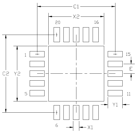
| Symbol | Millimeters |
|---|---|
| C1 | 4.0 |
| C2 | 4.0 |
| E | 0.50 BSC |
| X1 | 0.30 |
| X2 | 2.70 |
| Y1 | 0.80 |
| Y2 | 2.70 |
| Notes: General 1. All dimensions shown are in millimeters (mm) unless otherwise noted. 2. This land pattern design is based on IPC-7351 guidelines. Solder Mask Design 3. All metal pads are to be non-solder mask defined (NSMD). Clearance between the solder mask and the metal pad is to be 60 µm minimum, all the way around the pad. Stencil Design 4. A stainless steel, laser-cut and electro-polished stencil with trapezoidal walls should be used to assure good solder paste release. 5. The stencil thickness should be 0.125 mm (5 mils). 6. The ratio of stencil aperture to land pad size should be 1:1 for all perimeter pads. 7. A 2x2 array of 1.10 x 1.10 mm openings on 1.30 mm pitch should be used for the center ground pad. Card Assembly 8. A No-Clean, Type-3 solder paste is recommended. 9. The recommended card reflow profile is per the JEDEC/IPC J-STD-020 specification for Small Body components. | Notes: General 1. All dimensions shown are in millimeters (mm) unless otherwise noted. 2. This land pattern design is based on IPC-7351 guidelines. Solder Mask Design 3. All metal pads are to be non-solder mask defined (NSMD). Clearance between the solder mask and the metal pad is to be 60 µm minimum, all the way around the pad. Stencil Design 4. A stainless steel, laser-cut and electro-polished stencil with trapezoidal walls should be used to assure good solder paste release. 5. The stencil thickness should be 0.125 mm (5 mils). 6. The ratio of stencil aperture to land pad size should be 1:1 for all perimeter pads. 7. A 2x2 array of 1.10 x 1.10 mm openings on 1.30 mm pitch should be used for the center ground pad. Card Assembly 8. A No-Clean, Type-3 solder paste is recommended. 9. The recommended card reflow profile is per the JEDEC/IPC J-STD-020 specification for Small Body components. |
36 Skyworks Solutions, Inc. • Phone [781] 376-3000 • Fax [781] 376-3100 • [email protected] • www.skyworksinc.com
Rev. 1.3 • Skyworks Proprietary Information • Products and Product Information are Subject to Change Without Notice • August 27, 2021
Figure 27 shows the package details for the Si5351 in a 16-QFN package. Table 23 lists the values for the dimensions shown in the illustration.
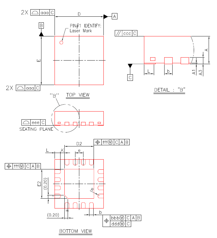
Skyworks Solutions, Inc. • Phone [781] 376-3000 • Fax [781] 376-3100 • [email protected] • www.skyworksinc.com 37 Rev. 1.3 • Skyworks Proprietary Information • Products and Product Information are Subject to Change Without Notice • August 27, 2021
A 0.80 0.85 0.90
A1 0.00 0.02 0.05
A3
b0.20 REF.
0.18
D
D2 0.25 0.30
3.0 BSC
1.70 1.80
e 0.50 BSC
E 3.0 BSC 1.90 E2 1.70 1.80 1.90
L 0.25 0.35 0.45
K 0.20 — —
R 0.09 — 0.14
aaa 0.15
bbb 0.10
ccc 0.10
ddd 0.05
eee 0.08
fff 0.10
Notes:
specification for Small Body Components.
38 Skyworks Solutions, Inc. • Phone [781] 376-3000 • Fax [781] 376-3100 • [email protected] • www.skyworksinc.com
Rev. 1.3 • Skyworks Proprietary Information • Products and Product Information are Subject to Change Without Notice • August 27, 2021
Figure 28 shows the recommended land pattern details for the Si5351 in a 16-Pin QFN package. Table 24 lists the values for the dimensions shown in the illustration.
Skyworks Solutions, Inc. • Phone [781] 376-3000 • Fax [781] 376-3100 • [email protected] • www.skyworksinc.com 39 Rev. 1.3 • Skyworks Proprietary Information • Products and Product Information are Subject to Change Without Notice • August 27, 2021
| Symbol | Millimeters |
|---|---|
| C1 | 3.00 |
| C2 | 3.00 |
| E | 0.50 |
| X1 | 0.30 |
| Y1 | 0.75 |
| X2 | 1.80 |
| Y2 | 1.80 |
| Notes: General 1. All dimensions shown are in millimeters (mm). 2. This land pattern design is based on IPC-7351 guidelines. 3. All dimensions shown are at Maximum Material Condition (MMC). Least Material Condition (LMC) is calculated based on a Fabrication Allowance of 0.05 mm. Solder Mask Design 4. All metal pads are to be non-solder mask defined (NSMD). Clearance between the solder mask and the metal pad is to be 60 µm minimum, all the way around the pad. Stencil Design 5. A stainless steel, laser-cut and electro-polished stencil with trapezoidal walls should be used to assure good solder paste release. 6. The stencil thickness should be 0.125 mm (5 mils). 7. The ratio of stencil aperture to land pad size should be 1:1 for all perimeter pads. 8. A 2x2 array of 0.65 mm square openings on a 0.90 mm pitch should be used for the center ground pad. Card Assembly 9. A No-Clean, Type-3 solder paste is recommended. 10. The recommended card reflow profile is per the JEDEC/IPC J-STD-020 specification for Small Body components. 11. The above notes and stencil design are shared as recommendations only. A customer or user may find it necessary to use different parameters and fine-tune their SMT process as required for their application and tooling. | Notes: General 1. All dimensions shown are in millimeters (mm). 2. This land pattern design is based on IPC-7351 guidelines. 3. All dimensions shown are at Maximum Material Condition (MMC). Least Material Condition (LMC) is calculated based on a Fabrication Allowance of 0.05 mm. Solder Mask Design 4. All metal pads are to be non-solder mask defined (NSMD). Clearance between the solder mask and the metal pad is to be 60 µm minimum, all the way around the pad. Stencil Design 5. A stainless steel, laser-cut and electro-polished stencil with trapezoidal walls should be used to assure good solder paste release. 6. The stencil thickness should be 0.125 mm (5 mils). 7. The ratio of stencil aperture to land pad size should be 1:1 for all perimeter pads. 8. A 2x2 array of 0.65 mm square openings on a 0.90 mm pitch should be used for the center ground pad. Card Assembly 9. A No-Clean, Type-3 solder paste is recommended. 10. The recommended card reflow profile is per the JEDEC/IPC J-STD-020 specification for Small Body components. 11. The above notes and stencil design are shared as recommendations only. A customer or user may find it necessary to use different parameters and fine-tune their SMT process as required for their application and tooling. |
40 Skyworks Solutions, Inc. • Phone [781] 376-3000 • Fax [781] 376-3100 • [email protected] • www.skyworksinc.com
Rev. 1.3 • Skyworks Proprietary Information • Products and Product Information are Subject to Change Without Notice • August 27, 2021
Figure 29 illustrates the package details for the Si5351 in a 10-pin MSOP package. Table 25 lists the values for the dimensions shown in the illustration.
Skyworks Solutions, Inc. • Phone [781] 376-3000 • Fax [781] 376-3100 • [email protected] • www.skyworksinc.com 41 Rev. 1.3 • Skyworks Proprietary Information • Products and Product Information are Subject to Change Without Notice • August 27, 2021
| Dimension | Min | Nom | Max |
|---|---|---|---|
| A | — | — | 1.10 |
| A1 | 0.00 | — | 0.15 |
| A2 | 0.75 | 0.85 | 0.95 |
| b | 0.17 | — | 0.33 |
| c | 0.08 | — | 0.23 |
| D | 3.00 BSC | 3.00 BSC | 3.00 BSC |
| E | 4.90 BSC | 4.90 BSC | 4.90 BSC |
| E1 | 3.00 BSC | 3.00 BSC | 3.00 BSC |
| e | 0.50 BSC | 0.50 BSC | 0.50 BSC |
| L | 0.40 | 0.60 | 0.80 |
| L2 | 0.25 BSC | 0.25 BSC | 0.25 BSC |
| q | 0 | — | 8 |
| aaa | — | — | 0.20 |
| bbb | — | — | 0.25 |
| ccc | — | — | 0.10 |
| ddd | — | — | 0.08 |
| Notes: 1. All dimensions shown are in millimeters (mm) unless otherwise noted. 2. Dimensioning and Tolerancing per ANSI Y14.5M-1994. 3. This drawing conforms to the JEDEC Solid State Outline MO-137, Variation C 4. Recommended card reflow profile is per the JEDEC/IPC J-STD-020 specification for Small Body Components. | Notes: 1. All dimensions shown are in millimeters (mm) unless otherwise noted. 2. Dimensioning and Tolerancing per ANSI Y14.5M-1994. 3. This drawing conforms to the JEDEC Solid State Outline MO-137, Variation C 4. Recommended card reflow profile is per the JEDEC/IPC J-STD-020 specification for Small Body Components. | Notes: 1. All dimensions shown are in millimeters (mm) unless otherwise noted. 2. Dimensioning and Tolerancing per ANSI Y14.5M-1994. 3. This drawing conforms to the JEDEC Solid State Outline MO-137, Variation C 4. Recommended card reflow profile is per the JEDEC/IPC J-STD-020 specification for Small Body Components. | Notes: 1. All dimensions shown are in millimeters (mm) unless otherwise noted. 2. Dimensioning and Tolerancing per ANSI Y14.5M-1994. 3. This drawing conforms to the JEDEC Solid State Outline MO-137, Variation C 4. Recommended card reflow profile is per the JEDEC/IPC J-STD-020 specification for Small Body Components. |
42 Skyworks Solutions, Inc. • Phone [781] 376-3000 • Fax [781] 376-3100 • [email protected] • www.skyworksinc.com
Rev. 1.3 • Skyworks Proprietary Information • Products and Product Information are Subject to Change Without Notice • August 27, 2021
Figure 30 shows the recommended land pattern details for the Si5351 in a 10-Pin MSOP package. Table 26 lists the values for the dimensions shown in the illustration.
Symbol Millimeters
Min Max C1 4.40 REF E 0.50 BSC G1 3.00 — X1 — 0.30 Y1 Z1 1.40 REF — 5.80
Notes: General
Material Condition (LMC) is calculated based on a Fabrication Allowance of 0.05mm. Solder Mask Design
between the solder mask and the metal pad is to be 60 µm minimum, all the way around the pad. Stencil Design
walls should be used to assure good solder paste release.
Card Assembly
020C specification for Small Body components.
Skyworks Solutions, Inc. • Phone [781] 376-3000 • Fax [781] 376-3100 • [email protected] • www.skyworksinc.com 43 Rev. 1.3 • Skyworks Proprietary Information • Products and Product Information are Subject to Change Without Notice • August 27, 2021
Mark Method: Laser Pin 1 Mark: Filled Circle = 0.50 mm Diameter
(Bottom-Left Corner) Font Size: 0.60 mm (24 mils) Line 1 Mark Format Device Part Number Si5351 Line 2 Mark Format: TTTTTT = Mfg Code* Manufacturing Code from the Assembly Purchase
Order Form. Line 3 Mark Format: YY = Year
WW = Work Week Assigned by the Assembly House. Corresponds to the year and work week of the assembly date. *Note: The code shown in the “TTTTTT” line does not correspond to the orderable part number or frequency plan. It is used
for package assembly quality tracking purposes only.
44 Skyworks Solutions, Inc. • Phone [781] 376-3000 • Fax [781] 376-3100 • [email protected] • www.skyworksinc.com
Rev. 1.3 • Skyworks Proprietary Information • Products and Product Information are Subject to Change Without Notice • August 27, 2021
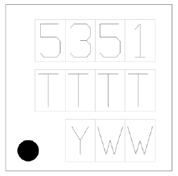
| Mark Method: | Laser | |
|---|---|---|
| Pin 1 Mark: | Circle (Bottom-Left Corner) | |
| Font Size: | 0.60 mm (24 mils) | |
| Line 1 Mark Format | Device Part Number | 5351 |
| Line 2 Mark Format: | TTTT = Mfg Code* | Manufacturing Code from the Assembly Purchase Order Form. |
| Line 3 Mark Format: | YWW = Date Code | Assigned by the Assembly House. Y = Last digit of the current year. WW = Work week of the assembly date. |
| *Note: The code shown in the “TTTT” line does not correspond to the orderable part number or frequency plan. It is used for package assembly quality tracking purposes only. | *Note: The code shown in the “TTTT” line does not correspond to the orderable part number or frequency plan. It is used for package assembly quality tracking purposes only. | *Note: The code shown in the “TTTT” line does not correspond to the orderable part number or frequency plan. It is used for package assembly quality tracking purposes only. |
Skyworks Solutions, Inc. • Phone [781] 376-3000 • Fax [781] 376-3100 • [email protected] • www.skyworksinc.com 45 Rev. 1.3 • Skyworks Proprietary Information • Products and Product Information are Subject to Change Without Notice • August 27, 2021
Mark Method: Laser Pin 1 Mark: Mold Dimple (Bottom-Left Corner) Font Size: 0.60 mm (24 mils) Line 1 Mark Format Device Part Number 5351 Line 2 Mark Format: TTTT = Mfg Code* Line 2 from the “Markings” section of the Assembly
Purchase Order form. Line 3 Mark Format: YWW = Date Code Assigned by the Assembly House.
Y = Last Digit of Current Year (Ex: 2013 = 3) WW = Work Week of Assembly Date. *Note: The code shown in the “TTTT” line does not correspond to the orderable part number or frequency plan. It is used for
package assembly quality tracking purposes only.
46 Skyworks Solutions, Inc. • Phone [781] 376-3000 • Fax [781] 376-3100 • [email protected] • www.skyworksinc.com
Rev. 1.3 • Skyworks Proprietary Information • Products and Product Information are Subject to Change Without Notice • August 27, 2021
March, 2020 Updated " Functional Block Diagrams" on page 2 with Si5351A 20-QFN and 16-QFN block diagrams. Updated "1. Ordering Guide" on page 4. Updated Table 4, “DC Characteristics,” on page 8 to include 16-QFN data. Updated thermal characteristics tables to include Table 10 (2-Layer Board), Table 11 (4-Layer Board), and Table 12 (Junction-to-Case). Updated "4.4. Spread Spectrum" on page 17. Added "4.6. Status Pins (INTR)" on page 17. Updated "5. I2C Interface" on page 18 with LSB pin option clarification. Updated "6. Configuring the Si5351" on page 20 with ClockBuilder Pro. Updated "6.3. Replacing Crystals and Crystal Oscillators" on page 22. Updated "6.7. HCSL Compatible Outputs" on page 24. Updated "8. Register Map Summary" on page 26. Updated "9. Register Descriptions" on page 26. Updated "10. Si5351 Pin Descriptions" on page 27 with 16-QFN pin descriptions and Ground Pad description. Updated "10.3. Si5351C 20-Pin QFN" on page 29. Updated Figure 24, “Device Part Numbers,” on page 34. Updated "11. Ordering Information" on page 34. Updated "12. Packaging" on page 35 with 16-QFN package information. Updated "13. Top Marking" on page 44 with 16-QFN top mark.
August, 2018 Updated "11. Ordering Information" on page 34.
Changed “Blank = Bulk” to “Blank = Coil Tape” in Figure 24.
April, 2015 Extended frequency range from 8 kHz-160 MHz to 2.5 kHz-200 MHz. Updated block diagrams for clarity. Added complete Si5350/1 family table, Table 1. Added top mark information. Added land pattern drawings. Added PowerUp Time, PLL Bypass mode, Table 4. Clarified Down Spread step sizes in Table 4. Updated max jitter specs (typ unchanged) in Table 6. Clarified power supply sequencing requirement, Section 6.2.
October, 2012 Initial release.
Skyworks Solutions, Inc. • Phone [781] 376-3000 • Fax [781] 376-3100 • [email protected] • www.skyworksinc.com 47 Rev. 1.3 • Skyworks Proprietary Information • Products and Product Information are Subject to Change Without Notice • August 27, 2021

Customize Skyworks clock generators, jitter attenuators and network synchronizers with a single tool. With CBPro you can control evaluation boards, access documentation, request a custom part number, export for in-system programming and more!
www.skyworksinc.com/CBPro Portfolio SW/HW Quality Support & Resources www.skyworksinc.com/ia/timing www.skyworksinc.com/CBPro www.skyworksinc.com/quality www.skyworksinc.com/support Copyright © 2021 Skyworks Solutions, Inc. All Rights Reserved. Information in this document is provided in connection with Skyworks Solutions, Inc. (“Skyworks”) products or services. These materials, including the information contained herein, are provided by Skyworks as a service to its customers and may be used for informational purposes only by the customer. Skyworks assumes no responsibility for errors or omissions in these materials or the information contained herein. Skyworks may change its documentation, products, services, specifications or product descriptions at any time, without notice. Skyworks makes no commitment to update the materials or information and shall have no responsibility whatsoever for conflicts, incompatibilities, or other difficulties arising from any future changes.
No license, whether express, implied, by estoppel or otherwise, is granted to any intellectual property rights by this document. Skyworks assumes no liability for any materials, products or information provided hereunder, including the sale, distribution, reproduction or use of Skyworks products, information or materials, except as may be provided in Skyworks’ Terms and Conditions of Sale.
THE MATERIALS, PRODUCTS AND INFORMATION ARE PROVIDED “AS IS” WITHOUT WARRANTY OF ANY KIND, WHETHER EXPRESS, IMPLIED, STATUTORY, OR OTHERWISE, INCLUDING FITNESS FOR A PARTICULAR PURPOSE OR USE, MERCHANTABILITY, PERFORMANCE, QUALITY OR NON-INFRINGEMENT OF ANY INTELLECTUAL PROPERTY RIGHT; ALL SUCH WARRANTIES ARE HEREBY EXPRESSLY DISCLAIMED. SKYWORKS DOES NOT WARRANT THE ACCURACY OR COMPLETENESS OF THE INFORMATION, TEXT, GRAPHICS OR OTHER ITEMS CONTAINED WITHIN THESE MATERIALS. SKYWORKS SHALL NOT BE LIABLE FOR ANY DAMAGES, INCLUDING BUT NOT LIMITED TO ANY SPECIAL, INDIRECT, INCIDENTAL, STATUTORY, OR CONSEQUENTIAL DAMAGES, INCLUDING WITHOUT LIMITATION, LOST REVENUES OR LOST PROFITS THAT MAY RESULT FROM THE USE OF THE MATERIALS OR INFORMATION, WHETHER OR NOT THE RECIPIENT OF MATERIALS HAS BEEN ADVISED OF THE POSSIBILITY OF SUCH DAMAGE.
Skyworks products are not intended for use in medical, lifesaving or life-sustaining applications, or other equipment in which the failure of the Skyworks products could lead to personal injury, death, physical or environmental damage. Skyworks customers using or selling Skyworks products for use in such applications do so at their own risk and agree to fully indemnify Skyworks for any damages resulting from such improper use or sale.
Customers are responsible for their products and applications using Skyworks products, which may deviate from published specifications as a result of design defects, errors, or operation of products outside of published parameters or design specifications. Customers should include design and operating safeguards to minimize these and other risks. Skyworks assumes no liability for applications assistance, customer product design, or damage to any equipment resulting from the use of Skyworks products outside of Skyworks’ published specifications or parameters.
Skyworks, the Skyworks symbol, Sky5 ® , SkyOne ® , SkyBlue™, Skyworks Green™, Clockbuilder ® , DSPLL ® , ISOmodem ® , ProSLIC ® , and SiPHY ® are trademarks or registered trademarks of Skyworks Solutions, Inc. or its subsidiaries in the United States and other countries. Third-party brands and names are for identification purposes only and are the property of their respective owners. Additional information, including relevant terms and conditions, posted at www.skyworksinc.com, are incorporated by reference.
Skyworks Solutions, Inc. | Nasdaq: SWKS | [email protected] | www.skyworksinc.com USA: 781-376-3000 | Asia: 886-2-2735 0399 | Europe: 33 (0)1 43548540 |