
⬇ Download Markdown · ⬇ Download LaTeX · ⬇ original · view original · CSV: table 1, table 2, table 3, table 4, table 5, table 6, table 7, table 8, table 9, table 10, table 11, table 12, table 13, table 14
The AP62300/AP62301/AP62300T is a 3A, synchronous buck converter with a wide input voltage range of 4.2V to 18V. The device fully integrates a 75mΩ high-side power MOSFET and a 45mΩ low-side power MOSFET to provide high-efficiency step-down DC-DC conversion. (Top View)
| The AP62300/AP62301/AP62300T device is easily used by minimizing | (Top View) | ||||
|---|---|---|---|---|---|
| the external component count due to its adoption of Constant On-Time | GND | 1 | 6 | BST | |
| (COT) control to achieve fast transient response, easy loop | VIN 1 6 FB | ||||
| stabilization, and low output-voltage ripple. | |||||
| SW 2 5 EN | SW | 2 | 5 | EN | |
The AP62300/AP62301/AP62300T design is optimized for Electromagnetic Interference (EMI) reduction. The device has a proprietary gate driver scheme to resist switching node ringing without sacrificing MOSFET turn-on and turn-off times, which reduces highfrequency radiated EMI noise caused by MOSFET switching.
VIN 1 6 FB SW 2 5 EN GND 3 4 BST SOT563 (Standard)
GND 1 6 BST SW 2 5 EN VIN 3 4 FB TSOT26 (Standard) The AP62300/AP62301 is available in SOT563 (Standard) and TSOT26 (Standard) packages. The AP62300T is available in a TSOT26 (Standard) package.
VIN: 4.2V to 18V Output Voltage (VOUT): 0.8V to 7V 3A Continuous Output Current 0.8V ± 1% Reference Voltage (T A = +25°C)
AP62300 and AP62301 0.763V ± 1% Reference Voltage (T A = +25°C)
AP62300T 155μA Low Quiescent Current (Pulse Frequency Modulation) 750kHz Switching Frequency (VIN = 12V, VOUT = 5V) Up to 83% Efficiency at 5mA Light Load Proprietary Gate Driver Design for Best EMI Reduction Protection Circuitry Undervoltage Lockout (UVLO) Cycle-by-Cycle Valley Current Limit Output Undervoltage Protection Thermal Shutdown Totally Lead-Free & Fully RoHS Compliant (Notes 1 & 2) Halogen and Antimony Free. “Green” Device (Note 3) For automotive applications requiring specific change control (i.e. parts qualified to AEC-Q100/101/104/200, PPAP capable, and manufactured in IATF 16949 certified facilities), please contact us or your local Diodes representative. https://www.diodes.com/quality/product-definitions/ Notes:
5V and 12V distributed power bus supplies Flat screen TV sets and monitors White goods and small home appliances FPGA, DSP, and ASIC supplies Home audios Network systems Gaming consoles Consumer electronics General purpose point of loads 1. No purposely added lead. Fully EU Directive 2002/95/EC (RoHS), 2011/65/EU (RoHS 2) & 2015/863/EU (RoHS 3) compliant. 2. See https://www.diodes.com/quality/lead-free/ for more information about Diodes Incorporated’s definitions of Halogen- and Antimony-free, "Green" and
Lead-free. 3. Halogen- and Antimony-free "Green” products are defined as those which contain <900ppm bromine, <900ppm chlorine (<1500ppm total Br + Cl) and
<1000ppm antimony compounds.
AP62300/AP62301/AP62300T Document number: DS41958 Rev. 4 - 2 1 of 23 www.diodes.com July 2023 © 2023 Copyright Diodes Incorporated. All Rights Reserved.

INTPUT
BST VIN
C6 EN L1
SW
OUTPUT
V OUT 5V
C5 Optional R1 FB C1 10μF C2 2x22μF R2 GND Figure 1. Typical Application Circuit VIN = 12V, VOUT = 5V, L = 3.3μH VIN = 12V, VOUT = 3.3V, L = 3.3μH 100 90 Efficiency (%)
80 70 60 50 40 30 20 10 0 0.001 0.010 0.100 1.000 10.000
IOUT (A)
Figure 2. Efficiency vs. Output Current, AP62300/AP62300T VIN = 12V, VOUT = 5V, L = 3.3μH VIN = 12V, VOUT = 3.3V, L = 3.3μH 100 90 Efficiency (%)
80 70 60 50 40 30 20 10 0 0.001 0.010 0.100 1.000 10.000
IOUT (A)
Figure 3. Efficiency vs. Output Current, AP62301 AP62300/AP62301/AP62300T Document number: DS41958 Rev. 4 - 2 2 of 23 www.diodes.com July 2023 © 2023 Copyright Diodes Incorporated. All Rights Reserved.

| Pin Name | Pin Number | Function | |
|---|---|---|---|
| Pin Name | SOT563 (Standard) | TSOT26 (Standard) | Function |
| VIN | 1 | 3 | Power Input. VIN supplies the power to the IC as well as the step-down converter power MOSFETs. Drive VIN with a 4.2V to 18V power source. Bypass VIN to GND with a suitably large capacitor to eliminate noise due to the switching of the IC. See Input Capacitor section for more details. |
| SW | 2 | 2 | Power Switching Output. SW is the switching node that supplies power to the output. Connect the output LC filter from SW to the output load. |
| GND | 3 | 1 | Power Ground. |
| BST | 4 | 6 | High-Side Gate Drive Boost Input. BST supplies the drive for the high-side N-Channel MOSFET. A 100nF capacitor or higher is recommended from BST to SW to power the high-side driver. |
| EN | 5 | 5 | Enable Input. EN is a digital input that turns the regulator on or off. Drive EN high to turn on the regulator and low to turn it off. Leave floating for automatic startup. The EN has a precision threshold of 1.2V for programing the UVLO. See Enable section for more details. |
| FB | 6 | 4 | Feedback sensing terminal for the output voltage. Connect this pin to the resistive divider of the output. See Setting the Output Voltage section for more details. |
I1 1.5µA EN I2 5.5µA 20kΩ
Minimum Off - Time S E Q1
UVP + + + -
0.763V FB S Q R Q Control Logic SW SW ZC On- Time Compute One- Shot VIN Thermal
Shutdown Q2 GND Figure 4. Functional Block Diagram AP62300/AP62301/AP62300T Document number: DS41958 Rev. 4 - 2 3 of 23 www.diodes.com July 2023 © 2023 Copyright Diodes Incorporated. All Rights Reserved.

| Symbol | Parameter | Rating | Unit | |
|---|---|---|---|---|
| VIN | Supply Pin Voltage | -0.3 to +20.0 (DC) | V | |
| VIN | Supply Pin Voltage | -0.3 to +22.0 (400ms) | V | |
| VSW | Switch Pin Voltage | -1.0 to VIN + 0.3 (DC) | V | |
| VSW | Switch Pin Voltage | -2.5 to VIN + 2.0 (20ns) | -2.5 to VIN + 2.0 (20ns) | V |
| VBST | Bootstrap Pin Voltage | VSW -0.3 to VSW + 6.0 | VSW -0.3 to VSW + 6.0 | V |
| VEN | Enable/UVLO Pin Voltage | -0.3 to +8.0 | -0.3 to +8.0 | V |
| VFB | Feedback Pin Voltage | -0.3 to +6.0 | -0.3 to +6.0 | V |
| TST | Storage Temperature | -65 to +150 | -65 to +150 | °C |
| TJ | Junction Temperature | +160 | +160 | °C |
| TL | Lead Temperature | +260 | +260 | °C |
| ESD Susceptibility (Note 5) | ESD Susceptibility (Note 5) | ESD Susceptibility (Note 5) | ESD Susceptibility (Note 5) | ESD Susceptibility (Note 5) |
| HBM | Human Body Model | ±2000 | ±2000 | V |
| CDM | Charged Device Model | ±500 | ±500 | V |
| Notes: 4. Stresses greater than the Absolute Maximum Ratings specified above can cause permanent damage to the device. These are stress ratings only; functional operation of the device at these or any other conditions exceeding those indicated in this specification is not implied. Device reliability can be affected by exposure to absolute maximum rating conditions for extended periods of time. 5. Semiconductor devices are ESD sensitive and can be damaged by exposure to ESD events. Suitable ESD precautions should be taken when handling and transporting these devices. Thermal Resistance (Note 6) Symbol Parameter Rating Unit | Notes: 4. Stresses greater than the Absolute Maximum Ratings specified above can cause permanent damage to the device. These are stress ratings only; functional operation of the device at these or any other conditions exceeding those indicated in this specification is not implied. Device reliability can be affected by exposure to absolute maximum rating conditions for extended periods of time. 5. Semiconductor devices are ESD sensitive and can be damaged by exposure to ESD events. Suitable ESD precautions should be taken when handling and transporting these devices. Thermal Resistance (Note 6) Symbol Parameter Rating Unit | Notes: 4. Stresses greater than the Absolute Maximum Ratings specified above can cause permanent damage to the device. These are stress ratings only; functional operation of the device at these or any other conditions exceeding those indicated in this specification is not implied. Device reliability can be affected by exposure to absolute maximum rating conditions for extended periods of time. 5. Semiconductor devices are ESD sensitive and can be damaged by exposure to ESD events. Suitable ESD precautions should be taken when handling and transporting these devices. Thermal Resistance (Note 6) Symbol Parameter Rating Unit | Notes: 4. Stresses greater than the Absolute Maximum Ratings specified above can cause permanent damage to the device. These are stress ratings only; functional operation of the device at these or any other conditions exceeding those indicated in this specification is not implied. Device reliability can be affected by exposure to absolute maximum rating conditions for extended periods of time. 5. Semiconductor devices are ESD sensitive and can be damaged by exposure to ESD events. Suitable ESD precautions should be taken when handling and transporting these devices. Thermal Resistance (Note 6) Symbol Parameter Rating Unit | Notes: 4. Stresses greater than the Absolute Maximum Ratings specified above can cause permanent damage to the device. These are stress ratings only; functional operation of the device at these or any other conditions exceeding those indicated in this specification is not implied. Device reliability can be affected by exposure to absolute maximum rating conditions for extended periods of time. 5. Semiconductor devices are ESD sensitive and can be damaged by exposure to ESD events. Suitable ESD precautions should be taken when handling and transporting these devices. Thermal Resistance (Note 6) Symbol Parameter Rating Unit |
| Notes: 4. Stresses greater than the Absolute Maximum Ratings specified above can cause permanent damage to the device. These are stress ratings only; functional operation of the device at these or any other conditions exceeding those indicated in this specification is not implied. Device reliability can be affected by exposure to absolute maximum rating conditions for extended periods of time. 5. Semiconductor devices are ESD sensitive and can be damaged by exposure to ESD events. Suitable ESD precautions should be taken when handling and transporting these devices. Thermal Resistance (Note 6) Symbol Parameter Rating Unit | Notes: 4. Stresses greater than the Absolute Maximum Ratings specified above can cause permanent damage to the device. These are stress ratings only; functional operation of the device at these or any other conditions exceeding those indicated in this specification is not implied. Device reliability can be affected by exposure to absolute maximum rating conditions for extended periods of time. 5. Semiconductor devices are ESD sensitive and can be damaged by exposure to ESD events. Suitable ESD precautions should be taken when handling and transporting these devices. Thermal Resistance (Note 6) Symbol Parameter Rating Unit | Notes: 4. Stresses greater than the Absolute Maximum Ratings specified above can cause permanent damage to the device. These are stress ratings only; functional operation of the device at these or any other conditions exceeding those indicated in this specification is not implied. Device reliability can be affected by exposure to absolute maximum rating conditions for extended periods of time. 5. Semiconductor devices are ESD sensitive and can be damaged by exposure to ESD events. Suitable ESD precautions should be taken when handling and transporting these devices. Thermal Resistance (Note 6) Symbol Parameter Rating Unit | Notes: 4. Stresses greater than the Absolute Maximum Ratings specified above can cause permanent damage to the device. These are stress ratings only; functional operation of the device at these or any other conditions exceeding those indicated in this specification is not implied. Device reliability can be affected by exposure to absolute maximum rating conditions for extended periods of time. 5. Semiconductor devices are ESD sensitive and can be damaged by exposure to ESD events. Suitable ESD precautions should be taken when handling and transporting these devices. Thermal Resistance (Note 6) Symbol Parameter Rating Unit | Notes: 4. Stresses greater than the Absolute Maximum Ratings specified above can cause permanent damage to the device. These are stress ratings only; functional operation of the device at these or any other conditions exceeding those indicated in this specification is not implied. Device reliability can be affected by exposure to absolute maximum rating conditions for extended periods of time. 5. Semiconductor devices are ESD sensitive and can be damaged by exposure to ESD events. Suitable ESD precautions should be taken when handling and transporting these devices. Thermal Resistance (Note 6) Symbol Parameter Rating Unit |
| θJA | Junction to Ambient | SOT563 (Standard) | 110 | °C/W |
| θJA | Junction to Ambient | TSOT26 (Standard) | 70 | °C/W |
| θJC | Junction to Case | SOT563 (Standard) | 8 | °C/W |
| θJC | Junction to Case | TSOT26 (Standard) | 12 | °C/W |
| Note: 6. Test condition for SOT563 (Standard)/TSOT26 (Standard): Device mounted on FR-4 substrate, two-layer PCB, 2oz copper, with minimum recommended pad layout. Recommended Operating Conditions (Note 7) (@ TA = +25°C, unless otherwise specified.) Symbol Parameter Min Max Unit | Note: 6. Test condition for SOT563 (Standard)/TSOT26 (Standard): Device mounted on FR-4 substrate, two-layer PCB, 2oz copper, with minimum recommended pad layout. Recommended Operating Conditions (Note 7) (@ TA = +25°C, unless otherwise specified.) Symbol Parameter Min Max Unit | Note: 6. Test condition for SOT563 (Standard)/TSOT26 (Standard): Device mounted on FR-4 substrate, two-layer PCB, 2oz copper, with minimum recommended pad layout. Recommended Operating Conditions (Note 7) (@ TA = +25°C, unless otherwise specified.) Symbol Parameter Min Max Unit | Note: 6. Test condition for SOT563 (Standard)/TSOT26 (Standard): Device mounted on FR-4 substrate, two-layer PCB, 2oz copper, with minimum recommended pad layout. Recommended Operating Conditions (Note 7) (@ TA = +25°C, unless otherwise specified.) Symbol Parameter Min Max Unit | Note: 6. Test condition for SOT563 (Standard)/TSOT26 (Standard): Device mounted on FR-4 substrate, two-layer PCB, 2oz copper, with minimum recommended pad layout. Recommended Operating Conditions (Note 7) (@ TA = +25°C, unless otherwise specified.) Symbol Parameter Min Max Unit |
| Note: 6. Test condition for SOT563 (Standard)/TSOT26 (Standard): Device mounted on FR-4 substrate, two-layer PCB, 2oz copper, with minimum recommended pad layout. Recommended Operating Conditions (Note 7) (@ TA = +25°C, unless otherwise specified.) Symbol Parameter Min Max Unit | Note: 6. Test condition for SOT563 (Standard)/TSOT26 (Standard): Device mounted on FR-4 substrate, two-layer PCB, 2oz copper, with minimum recommended pad layout. Recommended Operating Conditions (Note 7) (@ TA = +25°C, unless otherwise specified.) Symbol Parameter Min Max Unit | Note: 6. Test condition for SOT563 (Standard)/TSOT26 (Standard): Device mounted on FR-4 substrate, two-layer PCB, 2oz copper, with minimum recommended pad layout. Recommended Operating Conditions (Note 7) (@ TA = +25°C, unless otherwise specified.) Symbol Parameter Min Max Unit | Note: 6. Test condition for SOT563 (Standard)/TSOT26 (Standard): Device mounted on FR-4 substrate, two-layer PCB, 2oz copper, with minimum recommended pad layout. Recommended Operating Conditions (Note 7) (@ TA = +25°C, unless otherwise specified.) Symbol Parameter Min Max Unit | Note: 6. Test condition for SOT563 (Standard)/TSOT26 (Standard): Device mounted on FR-4 substrate, two-layer PCB, 2oz copper, with minimum recommended pad layout. Recommended Operating Conditions (Note 7) (@ TA = +25°C, unless otherwise specified.) Symbol Parameter Min Max Unit |
| VIN | Supply Voltage | 4.2 | 18.0 | V |
| VOUT | Output Voltage | 0.8 | 7.0 | V |
| TA | Operating Ambient Temperature | -40 | +85 | °C |
| TJ | Operating Junction Temperature | -40 | +125 | °C |
AP62300/AP62301/AP62300T Document number: DS41958 Rev. 4 - 2 4 of 23 www.diodes.com July 2023 © 2023 Copyright Diodes Incorporated. All Rights Reserved.

Electrical Characteristics (@ T J = +25°C, VIN = 12V, unless otherwise specified. Min/Max limits apply across the recommended operating junction temperature range, -40°C to +125°C, and input voltage range, 4.2V to 18V, unless otherwise specified.)
Symbol I SHDN Parameter Shutdown Supply Current Conditions Min
— Typ 1.5 Max — Unit μA
— 155 — μA
— — — — 275 3.90 3.6 75 — 4.15 — — μA V V mΩ Quiescent Supply Current V EN = 0V AP62300/AP62300T:
POR UVLO R DS(ON)1 VIN Power-On Reset Rising Threshold VIN Undervoltage Lockout Falling Threshold High-Side Power MOSFET On-Resistance (Note 8)
| Symbol | Parameter | Conditions | Min | Typ | Max | Unit |
|---|---|---|---|---|---|---|
| ISHDN | Shutdown Supply Current | VEN = 0V | — | 1.5 | — | μA |
| IQ | Quiescent Supply Current | AP62300/AP62300T: VFB = 0.85V | — | 155 | — | μA |
| IQ | Quiescent Supply Current | AP62301: VFB = 0.85V | — | 275 | — | μA |
| POR | VIN Power-On Reset Rising Threshold | — | — | 3.90 | 4.15 | V |
| UVLO | VIN Undervoltage Lockout Falling Threshold | — | — | 3.6 | — | V |
| RDS(ON)1 | High-Side Power MOSFET On-Resistance (Note 8) | — | — | 75 | — | mΩ |
| RDS(ON)2 | Low-Side Power MOSFET On-Resistance (Note 8) | — | — | 45 | — | mΩ |
| IVALLEY_LIMIT | LS Valley Current Limit (Note 8) | From Source to Drain | 3.2 | 3.7 | 4.2 | A |
| fSW | Oscillator Frequency | VOUT = 5V, CCM | — | 750 | — | kHz |
| tON_MIN | Minimum On-Time | — | — | 90 | — | ns |
| tOFF_MIN | Minimum Off-Time | — | — | 220 | — | ns |
| VFB | Feedback Voltage | AP62300/AP62301: TA = +25°C, CCM | 0.792 | 0.800 | 0.808 | V |
| VFB | Feedback Voltage | AP62300/AP62301: CCM | 0.784 | 0.800 | 0.816 | V |
| VFB | Feedback Voltage | AP62300T: TA = +25°C, CCM | 0.755 | 0.763 | 0.770 | V |
| VFB | Feedback Voltage | AP62300T: CCM | 0.747 | 0.763 | 0.778 | V |
| VEN_H | EN Logic High Threshold | — | — | 1.20 | 1.25 | V |
| VEN_L | EN Logic Low Threshold | — | 1.04 | 1.10 | — | V |
| IEN | EN Input Current | VEN = 1.5V | — | 7.0 | — | μA |
| IEN | EN Input Current | VEN = 1V | 1.0 | 1.5 | 2.0 | μA |
| tSS | Soft-Start Time | — | — | 2.5 | — | ms |
| TSD | Thermal Shutdown (Note 8) | — | — | +160 | — | °C |
| THys | Thermal Shutdown Hysteresis (Note 8) | — | — | +20 | — | °C |
AP62300/AP62301: CCM AP62300T:
AP62300T: CCM — V EN_L EN Logic Low Threshold — 1.04 1.10 — V
Feedback Voltage V FB Note:
I EN EN Input Current
t SS Soft-Start Time — — 2.5 — ms T SD Thermal Shutdown (Note 8) — — +160 — °C T Hys Thermal Shutdown Hysteresis (Note 8) — — +20 — °C
AP62300/AP62301/AP62300T Document number: DS41958 Rev. 4 - 2 5 of 23 www.diodes.com July 2023 © 2023 Copyright Diodes Incorporated. All Rights Reserved.

Typical Performance Characteristics (AP62300/AP62301/AP62300T @ T A = +25°C, VIN = 12V, VOUT = 5V, BOM = Table 1, unless otherwise specified.)
High-Side MOSFET 0.808 Low-Side MOSFET 0.804 0.802 V FB (V)
RDS(ON)
(mΩ)
0.806 120 110 100 90 80 70 60 50 40 30 20 0.800 0.798 0.796 0.794 0.792 0.790 0.788 -50 -25 0 25 50 75 100 125 -50 150 -25 0 50 75 100 125 150 Figure 6. Feedback Voltage vs. Temperature, AP62300/AP62301 0.774 5.0 0.772 4.5 0.770 4.0 0.768 3.5 I SHDN (μA)
VFB (V)
Figure 5. Power MOSFET R DS(ON) vs. Temperature 0.766 0.764 0.762 3.0 2.5 2.0 0.760 1.5 0.758 1.0 0.756 0.5 0.754 0.0
-50 -25 0 25 50 75 100 125 150
Temperature (°C)
VIN Rising POR -50 -25 0 25 50 75 100 125 150
Temperature (°C)
Figure 7. Feedback Voltage vs. Temperature, AP62300T VIN (V)
25 Temperature (°C) Temperature (°C)
Figure 8. I SHDN vs. Temperature VIN Falling UVLO
4.2 4.1 4.0 3.9 3.8 3.7 3.6 3.5 3.4 3.3 3.2
-50 -25 0 25 50 75 100 125 150
Temperature (°C)
Figure 9. VIN Power-On Reset and UVLO vs. Temperature AP62300/AP62301/AP62300T Document number: DS41958 Rev. 4 - 2 6 of 23 www.diodes.com July 2023 © 2023 Copyright Diodes Incorporated. All Rights Reserved.

Typical Performance Characteristics (AP62300/AP62301/AP62300T @ T A = +25°C, VIN = 12V, VOUT = 5V, BOM = Table 1, unless otherwise specified.) (continued)
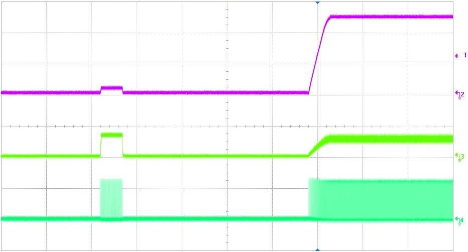
AP62300/AP62301/AP62300T Document number: DS41958 Rev. 4 - 2 7 of 23 www.diodes.com July 2023 © 2023 Copyright Diodes Incorporated. All Rights Reserved.

Typical Performance Characteristics (AP62300/AP62300T @ T A = +25°C, VIN = 12V, VOUT = 5V, BOM = Table 1, unless otherwise specified.)
VOUT (V)
100 95 90 85 80 75 70 65 60 55 50 0.001
0.010 0.100 1.000 IOUT = 0A IOUT = 1A
IOUT = 2A IOUT = 3A
5.50 5.25 5.00 4.75 4.50 4.25 4.00 3.75 3.50 3.25 3.00 4 10.000 6 8 10 12 14 16 IOUT (A) VIN (V)
Figure 14. Efficiency vs. Output Current, VIN = 12V Figure 15. Line Regulation 5.08 210 5.06 200 5.04 190 5.02 180 5.00 170 I Q (μA) VOUT (V)
Efficiency (%)
4.98 4.96 20 125 150 160 150 4.94 140 4.92 130 4.90 120 4.88 18 110 0.0 0.5 1.0 1.5 2.0 2.5 3.0 3.5 4.0 -50 -25 0 25 50 75 100
IOUT (A) Temperature (°C)
Figure 16. Load Regulation Figure 17. I Q vs. Temperature 1000
8 of 23 www.diodes.com July 2023 © 2023 Copyright Diodes Incorporated. All Rights Reserved.

Typical Performance Characteristics (AP62300/AP62300T @ T A = +25°C, VIN = 12V, VOUT = 5V, BOM = Table 1, unless otherwise specified.) (continued)
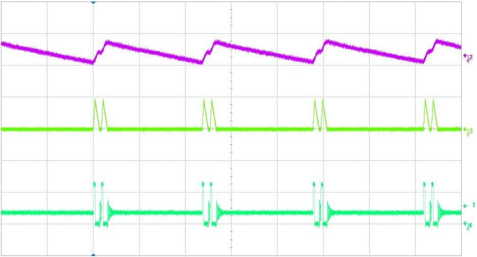
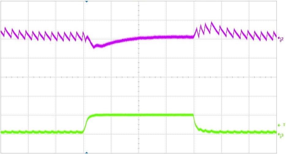
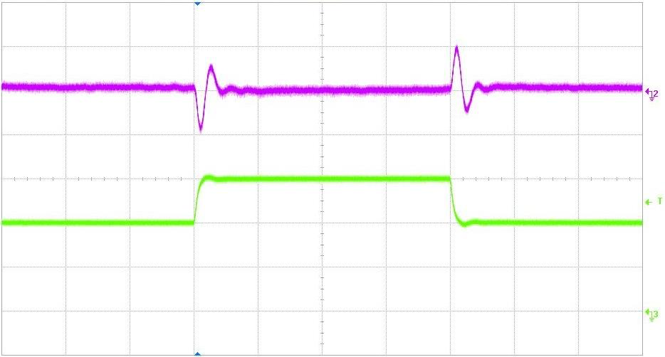
AP62300/AP62301/AP62300T Document number: DS41958 Rev. 4 - 2 9 of 23 www.diodes.com July 2023 © 2023 Copyright Diodes Incorporated. All Rights Reserved.

Typical Performance Characteristics (AP62301 @ T A = +25°C, VIN = 12V, VOUT = 5V, BOM = Table 1, unless otherwise specified.)
VOUT (V)
100 90 80 70 60 50 40 30 20 10 0 0.001
0.010 0.100 1.000 IOUT = 1A
IOUT = 2A IOUT = 3A
5.50 5.25 5.00 4.75 4.50 4.25 4.00 3.75 3.50 3.25 3.00 4 10.000 6 8 10 12 14 16
VIN (V)
Figure 26. Efficiency vs. Output Current, VIN = 12V Figure 27. Line Regulation 5.08 340 5.06 330 5.04 320 5.02 310 5.00 300 4.98 4.96 18 20 125 150 290 280 4.94 270 4.92 260 4.90 250 240 4.88
0.0 0.5 1.0 1.5 2.0 2.5 3.0 3.5 -50 4.0 -25 0 25 50 75 100
IOUT (A) Temperature (°C)
Figure 28. Load Regulation Figure 29. I Q vs. Temperature 800 790 780 770 760 750 740 730 720 710 700 1000 900 800 700 f SW (kHz)
fSW
IOUT = 0A IOUT (A)
IQ (μA) VOUT (V)
Efficiency (%)
600 500 400 300 200 100 -50 -25 0 25 50 75 100 125 150 0 0.010 0.100 1.000
Figure 30. f SW vs. Temperature, IOUT = 0A Figure 31. f SW vs. Load AP62300/AP62301/AP62300T Document number: DS41958 Rev. 4 - 2 10 of 23 www.diodes.com 10.000 July 2023 © 2023 Copyright Diodes Incorporated. All Rights Reserved.

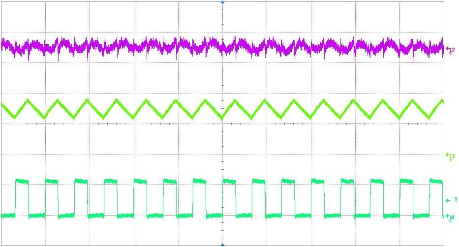
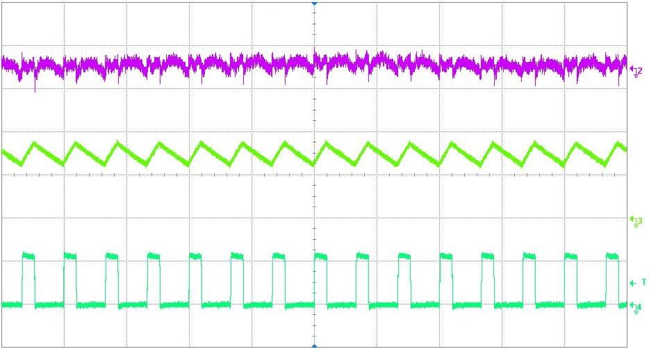
Typical Performance Characteristics (AP62301 @ T A = +25°C, VIN = 12V, VOUT = 5V, BOM = Table 1, unless otherwise specified.) (continued)
AP62300/AP62301/AP62300T Document number: DS41958 Rev. 4 - 2 11 of 23 www.diodes.com July 2023 © 2023 Copyright Diodes Incorporated. All Rights Reserved.

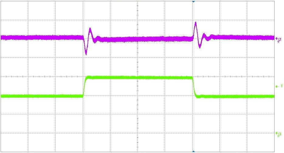
Typical Performance Characteristics (AP62301 @ T A = +25°C, VIN = 12V, VOUT = 5V, BOM = Table 1, unless otherwise specified.) (continued)
AP62300/AP62301/AP62300T Document number: DS41958 Rev. 4 - 2 12 of 23 www.diodes.com July 2023 © 2023 Copyright Diodes Incorporated. All Rights Reserved.

1 Pulse Width Modulation (PWM) Operation The AP62300/AP62301/AP62300T device is a 4.2V-to-18V input, 3A output, EMI friendly, fully integrated synchronous buck converter. Refer to the block diagram in Figure 4. The device employs constant on-time control to provide fast transient response and easy loop stabilization. At the beginning of each cycle, the one-shot pulse turns on the high-side power MOSFET, Q1, for a fixed on-time, t ON . This one-shot on-pulse timing is calculated by the converter’s input voltage and output voltage to maintain a pseudo-fixed frequency over the input voltage range. When Q1 is on, the inductor current rises linearly and the device charges the output capacitor. Q1 turns off after the fixed on-time expires, and the low-side power MOSFET, Q2, turns on. Once the output voltage drops below the output regulation, Q2 turns off. The one-shot timer is then reset and Q1 turns on again. The on-time is inversely proportional to the input voltage and directly proportional to the output voltage. It is calculated by the following equation:
Where: VIN is the input voltage VOUT is the output voltage f SW is the switching frequency The off-time duration is t OFF and starts after the on-time expires. The off-time expires when the feedback voltage decreases below the reference voltage, which then triggers the on-time duration to start again. The minimum off-time is 220ns typical.
In order to provide a small output ripple during light load conditions, the AP62301 operates in PWM regardless of output load.
2 Pulse Frequency Modulation (PFM) Operation The AP62300/AP62300T enters PFM operation at light load conditions for high efficiency. During light load conditions, the regulator automatically reduces the switching frequency. As the output current decreases, so too does the inductor current. The inductor current, I L , eventually reaches 0A, marking the boundary between Continuous Conduction Mode (CCM) and Discontinuous Condition Mode (DCM). During this time, both Q1 and Q2 are off, and the load current is provided only by the output capacitor. When V FB becomes lower than 0.8V for AP62300 or 0.763V for AP62300T, the next cycle begins, and Q1 turns on. Because the AP62300/AP62300T works in PFM during light load conditions, it can achieve power efficiency of up to 83% at a 5mA load condition.
Likewise, as the output load increases from light load to heavy load, the switching frequency increases to maintain the regulation of the output voltage. The transition point between light and heavy load conditions can be calculated using the following equation:
Where: L is the inductor value The quiescent current of AP62300/AP62300T is 155μA typical under a no-load, non-switching condition.
3 Enable When disabled, the device shutdown supply current is only 1.5μA. When applying a voltage greater than the EN logic high threshold (typical 1.2V, rising), the AP62300/AP62301/AP62300T enables all functions and the device initiates the soft-start phase. An internal 1.5µA pull-up current source connected from the internal LDO-regulated VCC to the EN pin guarantees that if EN is left floating, the device still automatically enables once the voltage reaches the EN logic high threshold. The AP62300/AP62301/AP62300T has a built-in 2.5ms soft-start time to prevent output voltage overshoot and inrush current. When the EN voltage falls below its logic low threshold (typical 1.1V, falling), the internal SS voltage discharges to ground and device operation disables.
The EN pin can also be used to program the undervoltage lockout thresholds. See Undervoltage Lockout (UVLO) section for more details.
AP62300/AP62301/AP62300T Document number: DS41958 Rev. 4 - 2 13 of 23 www.diodes.com July 2023 © 2023 Copyright Diodes Incorporated. All Rights Reserved.

3 Enable (continued)
Alternatively, a small ceramic capacitor can be added from EN to GND. When EN is not driven externally, this capacitor increases the time needed for the EN pin voltage to reach its logic high threshold, which delays the startup of the output voltage. This is useful when sequencing multiple power rails to minimize input inrush current. When the EN pin voltage starts from 0V, the amount of capacitance for a given delay time is approximated by:
Where: C d is the time delay capacitance in nF t d is the delay time in ms 4 Electromagnetic Interference (EMI) Reduction with Ringing-Free Switching Node In some applications, the system must meet EMI standards. In relation to high frequency radiation EMI noise, the switching node’s (SW’s) ringing amplitude is especially critical. To dampen high frequency radiated EMI noise, the AP62300/AP62301/AP62300T device implements a proprietary, multi-level gate driver scheme that achieves a ringing-free switching node without sacrificing the switching node’s rise and fall slew rates as well as the converter’s power efficiency.
5 Adjusting Undervoltage Lockout (UVLO)
Undervoltage lockout is implemented to prevent the IC from insufficient input voltages. The AP62300/AP62301/AP62300T device has a UVLO comparator that monitors the input voltage and the internal bandgap reference. The AP62300/AP62301/AP62300T disables if the input voltage falls below 3.6V. In this UVLO event, both the high-side and low-side power MOSFETs turn off.
Some applications may desire higher VIN UVLO threshold voltages than is provided by the default setup. A 5.5µA hysteresis pull-up current source on the EN pin along with an external resistive divider (R3 and R4) configures the VIN UVLO threshold voltages as shown in Figure 39.
Figure 39. Programming UVLO The resistive divider resistor values are calculated by:
Where: V ON is the rising edge VIN voltage to enable the regulator and is greater than 4.15V V OFF is the falling edge VIN voltage to disable the regulator and is greater than 3.85V AP62300/AP62301/AP62300T Document number: DS41958 Rev. 4 - 2 14 of 23 www.diodes.com July 2023 © 2023 Copyright Diodes Incorporated. All Rights Reserved.

6 Overcurrent Protection (OCP)
The AP62300/AP62301/AP62300T has cycle-by-cycle valley current limit protection by sensing the current through the internal low-side power MOSFET, Q2. While Q2 is on, the internal sensing circuitry monitors its conduction current. The overcurrent limit has a corresponding voltage limit, V LIMIT . When the voltage between GND and SW is lower than V LIMIT due to excessive current through Q2, the OCP triggers, and the controller turns off Q2. During this time, both Q1 and Q2 remain off. A new switching cycle begins only when the voltage between GND and SW rises above V LIMIT . If Q2 consistently hits the valley current limit for 2.5ms or the VFB is less than 495mV (UVP threshold), the buck converter enters hiccup mode and shuts down. After 20ms of down time, the buck converter restarts powering up. Hiccup mode reduces the power dissipation in the overcurrent condition.
Because the R DS(ON) values of the power MOSFETs increase with temperature, V LIMIT has a temperature coefficient of 0.4%/°C to compensate for the temperature dependency of R DS(ON) .
7 Thermal Shutdown (TSD)
If the junction temperature of the device reaches the thermal shutdown limit of +160°C, the AP62300/AP62301/AP62300T shuts down both its highside and low-side power MOSFETs. When the junction temperature reduces to the required level (+140°C typical), the device initiates a normal power-up cycle with soft-start.
8 Power Derating Characteristics To prevent the regulator from exceeding the maximum recommended operating junction temperature, some thermal analysis is required. The regulator’s temperature rise is given by:
Where: PD is the power dissipated by the regulator θ JA is the thermal resistance from the junction of the die to the ambient temperature The junction temperature, T J , is given by:
Where: T A is the ambient temperature of the environment AP62300/AP62301/AP62300T Document number: DS41958 Rev. 4 - 2 15 of 23 www.diodes.com July 2023 © 2023 Copyright Diodes Incorporated. All Rights Reserved.

8 Power Derating Characteristics (continued)
For the SOT563 (Standard) and TSOT26 (Standard) packages, the θ JA is 110°C/W and 70°C/W, respectively. The actual junction temperature should not exceed the maximum recommended operating junction temperature of +125°C when considering the thermal design. Figure 40 and Figure 41 show typical derating curves versus ambient temperature.
VOUT = 1.2V VOUT = 1.5V VOUT = 1.8V
VOUT = 2.5V VOUT = 3.3V VOUT = 5V
5.0 4.5 4.0 IOUT (A)
3.5 3.0 2.5 2.0 1.5 1.0 0.5 0.0
0 20 40 60 80 100 120 140 160
Ambient Temperature (°C)
Figure 40. Output Current Derating Curve vs. Ambient Temperature, SOT563 (Standard) Package, VIN = 12V VOUT = 1.2V VOUT = 1.5V VOUT = 1.8V
VOUT = 2.5V VOUT = 3.3V VOUT = 5V
5.0 4.5 4.0 IOUT (A)
3.5 3.0 2.5 2.0 1.5 1.0 0.5 0.0
0 20 40 60 80 100 120 140 160
Ambient Temperature (°C)
Figure 41. Output Current Derating Curve vs. Ambient Temperature, TSOT26 (Standard) Package, VIN = 12V AP62300/AP62301/AP62300T Document number: DS41958 Rev. 4 - 2 16 of 23 www.diodes.com July 2023 © 2023 Copyright Diodes Incorporated. All Rights Reserved.

9 Setting the Output Voltage The AP62300/AP62301/AP62300T has adjustable output voltages, starting from 0.8V for AP62300/AP62301 and 0.763V for AP62300T, using an external resistive divider. The resistor values of the feedback network are selected based on a design trade-off between efficiency and output voltage accuracy. There is less current consumption in the feedback network for high resistor values, which improves efficiency at light loads. However, values too high cause the device to be more susceptible to noise affecting its output voltage accuracy. R1 can be determined by the following equation:
Eq. 8 Where: V FB is the feedback voltage Table 1 shows a list of recommended component selections for common AP62300/AP62301/AP62300T output voltages referencing Figure 1. Consult Diodes Incorporated for other output voltage requirements.
Table 1. Recommended Component Selections
AP62300/AP62301/AP62300T Output Voltage (V)
1.2 1.5 1.8 2.5 3.3 5.0 10 AP62300/AP62301
R1 (kΩ)
| AP62300/AP62301/AP62300T | ||||||||
|---|---|---|---|---|---|---|---|---|
| Output Voltage (V) | AP62300/AP62301R1 (kΩ) | AP62300TR1 (kΩ) | R2 (kΩ) | L (µH) | C1 (µF) | C2 (µF) | C5 (pF) (Optional) | C6 (nF) |
| 1.2 | 4.99 | 5.76 | 10 | 1.5 | 10 | 2 x 22 | Open | 100 |
| 1.5 | 8.66 | 9.76 | 10 | 1.5 | 10 | 2 x 22 | Open | 100 |
| 1.8 | 12.4 | 13.7 | 10 | 2.2 | 10 | 2 x 22 | 10 -100 | 100 |
| 2.5 | 21.5 | 22.6 | 10 | 2.2 | 10 | 2 x 22 | 10 -100 | 100 -220 |
| 3.3 | 31.6 | 33.2 | 10 | 3.3 | 10 | 2 x 22 | 10 -100 | 100 -330 |
| 5.0 | 52.3 | 56.2 | 10 | 3.3 | 10 | 2 x 22 | 10 -100 | 100 -330 |
100 100 100 100 - 220 100 - 330 100 - 330 Inductor Calculating the inductor value is a critical factor in designing a buck converter. For most designs, the following equation can be used to calculate the inductor value:
Where: ∆I L is the inductor current ripple f SW is the buck converter switching frequency For AP62300/AP62301/AP62300T, choose ∆I L to be 30% to 50% of the maximum load current of 3A.
The inductor peak current is calculated by:
Eq. 10 Peak current determines the required saturation current rating, which influences the size of the inductor. Saturating the inductor decreases the converter efficiency while increasing the temperatures of the inductor and the internal power MOSFETs. Therefore, choosing an inductor with the appropriate saturation current rating is important. For most applications, it is recommended to select an inductor of approximately 1.2µH to 4.7µH with a DC current rating of at least 35% higher than the maximum load current. For highest efficiency, the inductor’s DC resistance should be less than 30mΩ. Use a larger inductance for improved efficiency under light load conditions.
AP62300/AP62301/AP62300T Document number: DS41958 Rev. 4 - 2 17 of 23 www.diodes.com July 2023 © 2023 Copyright Diodes Incorporated. All Rights Reserved.

11 Input Capacitor The input capacitor reduces both the surge current drawn from the input supply as well as the switching noise from the device. The input capacitor must sustain the ripple current produced during the on-time of Q1. It must have a low ESR to minimize power dissipation due to the RMS input current.
The RMS current rating of the input capacitor is a critical parameter and must be higher than the RMS input current. As a rule of thumb, select an input capacitor with an RMS current rating greater than half of the maximum load current.
Due to large dI/dt through the input capacitor, electrolytic or ceramic capacitors with low ESR should be used. If using a tantalum capacitor, it must be surge protected or else capacitor failure could occur. Using a ceramic capacitor of 10µF or greater is sufficient for most applications.
12 Output Capacitor The output capacitor keeps the output voltage ripple small, ensures feedback loop stability, and reduces both the overshoots and undershoots of the output voltage during load transients. During the first few microseconds of an increasing load transient, the converter recognizes the change from steady-state and sets the off-time to minimum to supply more current to the load. However, the inductor limits the change to increasing current depending on its inductance. Therefore, the output capacitor supplies the difference in current to the load during this time. Likewise, during the first few microseconds of a decreasing load transient, the converter recognizes the change from steady-state and increases the off-time to reduce the current supplied to the load. However, the inductor limits the change in decreasing current as well. Therefore, the output capacitor absorbs the excess current from the inductor during this time.
The effective output capacitance, COUT, requirements can be calculated from the equations below.
The ESR of the output capacitor dominates the output voltage ripple. The amount of ripple can be calculated by:
Eq. 11 An output capacitor with large capacitance and low ESR is the best option. For most applications, a 22µF to 68µF ceramic capacitor is sufficient. To meet the load transient requirements, the calculated COUT should satisfy the following inequality:
Where: I Trans is the load transient ∆V Overshoot is the maximum output overshoot voltage ∆V Undershoot is the maximum output undershoot voltage 13 Bootstrap Capacitor To ensure proper operation, a ceramic capacitor must be connected between the BST and SW pins to supply the drive voltage for the high-side power MOSFET. A 100nF ceramic capacitor is sufficient for most applications. In the cases where output voltage is higher than 2.5V, a higher capacitance recommended to help maintain stable voltage from BST to SW.
AP62300/AP62301/AP62300T Document number: DS41958 Rev. 4 - 2 18 of 23 www.diodes.com July 2023 © 2023 Copyright Diodes Incorporated. All Rights Reserved.

PCB Layout 1. The AP62300/AP62301/AP62300T works at 3A load current so heat dissipation is a major concern in the layout of the PCB. 2oz copper for
both the top and bottom layers is recommended.
R1 FB SW EN GND BST C2
GND BST SW EN VIN FB C3 C2
C1 VIN
C1
R1 R2
Figure 42. Recommended PCB Layout, SOT563 (Standard)
AP62300/AP62301/AP62300T Document number: DS41958 Rev. 4 - 2 Figure 43. Recommended PCB Layout, TSOT26 (Standard)
19 of 23 www.diodes.com July 2023 © 2023 Copyright Diodes Incorporated. All Rights Reserved.

Product Version Package Packing 0 : AP62300 1 : AP62301 0T : AP62300T Z6 : SOT563 (Standard) WU : TSOT26 (Standard)
| Part Number | Operation Mode | VFB (V) | Package Code | Tape and Reel | |
|---|---|---|---|---|---|
| Part Number | Operation Mode | VFB (V) | Package Code | Quantity | Part Number Suffix |
| AP62300Z6-7 | PFM/PWM | 0.800 | Z6 | 3000 | -7 |
| AP62300WU-7 | PFM/PWM | 0.800 | WU | 3000 | -7 |
| AP62301Z6-7 | PWM Only | 0.800 | Z6 | 3000 | -7 |
| AP62301WU-7 | PWM Only | 0.800 | WU | 3000 | -7 |
| AP62300TWU-7 | PFM/PWM | 0.763 | WU | 3000 | -7 |
| Marking Information SOT563 (Standard)/TSOT26 (Standard) ( Top View ) 6 5 7 4 XX : Identification Code Y : Year 0~9 XX Y W X W : Week : A~Z : 1~26 week; a~z : 27~52 week; z represents 1 2 3 X : 52 Internal and 53 Code week Part Number Package Identification Code | Marking Information SOT563 (Standard)/TSOT26 (Standard) ( Top View ) 6 5 7 4 XX : Identification Code Y : Year 0~9 XX Y W X W : Week : A~Z : 1~26 week; a~z : 27~52 week; z represents 1 2 3 X : 52 Internal and 53 Code week Part Number Package Identification Code | Marking Information SOT563 (Standard)/TSOT26 (Standard) ( Top View ) 6 5 7 4 XX : Identification Code Y : Year 0~9 XX Y W X W : Week : A~Z : 1~26 week; a~z : 27~52 week; z represents 1 2 3 X : 52 Internal and 53 Code week Part Number Package Identification Code | Marking Information SOT563 (Standard)/TSOT26 (Standard) ( Top View ) 6 5 7 4 XX : Identification Code Y : Year 0~9 XX Y W X W : Week : A~Z : 1~26 week; a~z : 27~52 week; z represents 1 2 3 X : 52 Internal and 53 Code week Part Number Package Identification Code | Marking Information SOT563 (Standard)/TSOT26 (Standard) ( Top View ) 6 5 7 4 XX : Identification Code Y : Year 0~9 XX Y W X W : Week : A~Z : 1~26 week; a~z : 27~52 week; z represents 1 2 3 X : 52 Internal and 53 Code week Part Number Package Identification Code | Marking Information SOT563 (Standard)/TSOT26 (Standard) ( Top View ) 6 5 7 4 XX : Identification Code Y : Year 0~9 XX Y W X W : Week : A~Z : 1~26 week; a~z : 27~52 week; z represents 1 2 3 X : 52 Internal and 53 Code week Part Number Package Identification Code |
| Marking Information SOT563 (Standard)/TSOT26 (Standard) ( Top View ) 6 5 7 4 XX : Identification Code Y : Year 0~9 XX Y W X W : Week : A~Z : 1~26 week; a~z : 27~52 week; z represents 1 2 3 X : 52 Internal and 53 Code week Part Number Package Identification Code | Marking Information SOT563 (Standard)/TSOT26 (Standard) ( Top View ) 6 5 7 4 XX : Identification Code Y : Year 0~9 XX Y W X W : Week : A~Z : 1~26 week; a~z : 27~52 week; z represents 1 2 3 X : 52 Internal and 53 Code week Part Number Package Identification Code | Marking Information SOT563 (Standard)/TSOT26 (Standard) ( Top View ) 6 5 7 4 XX : Identification Code Y : Year 0~9 XX Y W X W : Week : A~Z : 1~26 week; a~z : 27~52 week; z represents 1 2 3 X : 52 Internal and 53 Code week Part Number Package Identification Code | Marking Information SOT563 (Standard)/TSOT26 (Standard) ( Top View ) 6 5 7 4 XX : Identification Code Y : Year 0~9 XX Y W X W : Week : A~Z : 1~26 week; a~z : 27~52 week; z represents 1 2 3 X : 52 Internal and 53 Code week Part Number Package Identification Code | Marking Information SOT563 (Standard)/TSOT26 (Standard) ( Top View ) 6 5 7 4 XX : Identification Code Y : Year 0~9 XX Y W X W : Week : A~Z : 1~26 week; a~z : 27~52 week; z represents 1 2 3 X : 52 Internal and 53 Code week Part Number Package Identification Code | Marking Information SOT563 (Standard)/TSOT26 (Standard) ( Top View ) 6 5 7 4 XX : Identification Code Y : Year 0~9 XX Y W X W : Week : A~Z : 1~26 week; a~z : 27~52 week; z represents 1 2 3 X : 52 Internal and 53 Code week Part Number Package Identification Code |
| AP62300Z6-7 | AP62300Z6-7 | SOT563 (Standard) | SOT563 (Standard) | HE | HE |
| AP62300WU-7 | AP62300WU-7 | TSOT26 (Standard) | TSOT26 (Standard) | HF | HF |
| AP62301Z6-7 | AP62301Z6-7 | SOT563 (Standard) | SOT563 (Standard) | HX | HX |
| AP62301WU-7 | AP62301WU-7 | TSOT26 (Standard) | TSOT26 (Standard) | HY | HY |
| AP62300TWU-7 | AP62300TWU-7 | TSOT26 (Standard) | TSOT26 (Standard) | TP | TP |
20 of 23 www.diodes.com Identification Code
HE HF HX HY TP July 2023 © 2023 Copyright Diodes Incorporated. All Rights Reserved.

Please see http://www.diodes.com/package-outlines.html for the latest version.
SOT563 (Standard)
bE E1 e SOT563 (Standard) Dim Min Max Typ A 0.53 0.60 — b 0.15 0.30 0.20 c 0.10 0.18 0.11 D 1.50 1.70 1.60 E 1.50 1.70 1.60 E1 1.10 1.30 1.20 e 0.50 BSC L 0.10 0.30 0.20 All Dimensions in mm L D c A O P T IO N A O P T IO N B O P T IO N A O P T IO N B ( T O P V IE W ) ( T O P V IE W ) ( S I D E V IE W ) ( S I D E V IE W )
TSOT26 (Standard)
TSOT26 (Standard) Dim Min Max Typ A — 1.00 — A1 0.00 0.10 — A2 0.75 0.90 0.80 D 2.70 3.10 2.90 E 2.60 3.00 2.80 E1 1.50 1.70 1.60 b 0.30 0.50 0.44 c 0.11 0.20 0.16 e 0.95 BSC L 0.30 0.50 0.40 L2 0.25 BSC θ 0° 8° 4° All Dimensions in mm D E 1 /2
E /2 E 1 E
c
G a u g e P la n e 0
Lb e S e a tin g P la n e L2
A2
A1 A
S e a tin g P la n e O P T IO N A ( T O P V IE W )
O P T IO N B ( T O P V IE W )
AP62300/AP62301/AP62300T Document number: DS41958 Rev. 4 - 2 O P T IO N A ( S ID E V IE W )
21 of 23 www.diodes.com O P T IO N B ( S ID E V IE W )
July 2023 © 2023 Copyright Diodes Incorporated. All Rights Reserved.

Please see http://www.diodes.com/package-outlines.html for the latest version.
SOT563 (Standard)
C X Y Y1 G C1 Dimensions
CC1 G X X1 Y Y1 Value (in mm)
0.500 1.270 0.600 0.300 1.300 0.670 1.940 Dimensions
CX Y Y1 Value (in mm)
0.950 0.700 1.000 3.200 X1 TSOT26 (Standard)
CY1 Y X
SOT563 (Standard) Moisture Sensitivity: Level 1 per J-STD-020 Terminals: Finish – Matte Tin Plated Leads, Solderable per MIL-STD-202, Method 208 Weight: 0.003 grams (Approximate)
TSOT26 (Standard) Moisture Sensitivity: Level 1 per J-STD-020 Terminals: Finish – Matte Tin Plated Leads, Solderable per MIL-STD-202, Method 208 Weight: 0.013 grams (Approximate)
AP62300/AP62301/AP62300T Document number: DS41958 Rev. 4 - 2 22 of 23 www.diodes.com July 2023 © 2023 Copyright Diodes Incorporated. All Rights Reserved.

IMPORTANT NOTICE 1. DIODES INCORPORATED (Diodes) AND ITS SUBSIDIARIES MAKE NO WARRANTY OF ANY KIND, EXPRESS OR IMPLIED, WITH REGARDS TO ANY INFORMATION CONTAINED IN THIS DOCUMENT, INCLUDING, BUT NOT LIMITED TO, THE IMPLIED WARRANTIES OF MERCHANTABILITY, FITNESS FOR A PARTICULAR PURPOSE OR NON-INFRINGEMENT OF THIRD PARTY INTELLECTUAL PROPERTY RIGHTS (AND THEIR EQUIVALENTS UNDER THE LAWS OF ANY JURISDICTION).
The Information contained herein is for informational purpose only and is provided only to illustrate the operation of Diodes’ products described herein and application examples. Diodes does not assume any liability arising out of the application or use of this document or any product described herein. This document is intended for skilled and technically trained engineering customers and users who design with Diodes’ products. Diodes’ products may be used to facilitate safety-related applications; however, in all instances customers and users are responsible for (a) selecting the appropriate Diodes products for their applications, (b) evaluating the suitability of Diodes’ products for their intended applications, (c) ensuring their applications, which incorporate Diodes’ products, comply the applicable legal and regulatory requirements as well as safety and functionalsafety related standards, and (d) ensuring they design with appropriate safeguards (including testing, validation, quality control techniques, redundancy, malfunction prevention, and appropriate treatment for aging degradation) to minimize the risks associated with their applications.
Diodes assumes no liability for any application-related information, support, assistance or feedback that may be provided by Diodes from time to time. Any customer or user of this document or products described herein will assume all risks and liabilities associated with such use, and will hold Diodes and all companies whose products are represented herein or on Diodes’ websites, harmless against all damages and liabilities.
Products described herein may be covered by one or more United States, international or foreign patents and pending patent applications. Product names and markings noted herein may also be covered by one or more United States, international or foreign trademarks and trademark applications. Diodes does not convey any license under any of its intellectual property rights or the rights of any third parties (including third parties whose products and services may be described in this document or on Diodes’ website) under this document.
Diodes’ products are provided subject to Diodes’ Standard Terms and Conditions of Sale (https://www.diodes.com/about/company/terms-and-conditions/terms-and-conditions-of-sales/) or other applicable terms. This document does not alter or expand the applicable warranties provided by Diodes. Diodes does not warrant or accept any liability whatsoever in respect of any products purchased through unauthorized sales channel.
Diodes’ products and technology may not be used for or incorporated into any products or systems whose manufacture, use or sale is prohibited under any applicable laws and regulations. Should customers or users use Diodes’ products in contravention of any applicable laws or regulations, or for any unintended or unauthorized application, customers and users will (a) be solely responsible for any damages, losses or penalties arising in connection therewith or as a result thereof, and (b) indemnify and hold Diodes and its representatives and agents harmless against any and all claims, damages, expenses, and attorney fees arising out of, directly or indirectly, any claim relating to any noncompliance with the applicable laws and regulations, as well as any unintended or unauthorized application.
While efforts have been made to ensure the information contained in this document is accurate, complete and current, it may contain technical inaccuracies, omissions and typographical errors. Diodes does not warrant that information contained in this document is error-free and Diodes is under no obligation to update or otherwise correct this information. Notwithstanding the foregoing, Diodes reserves the right to make modifications, enhancements, improvements, corrections or other changes without further notice to this document and any product described herein. This document is written in English but may be translated into multiple languages for reference. Only the English version of this document is the final and determinative format released by Diodes.
Any unauthorized copying, modification, distribution, transmission, display or other use of this document (or any portion hereof) is prohibited. Diodes assumes no responsibility for any losses incurred by the customers or users or any third parties arising from any such unauthorized use.
This Notice may be periodically updated with the most recent version available at https://www.diodes.com/about/company/terms-andconditions/important-notice The Diodes logo is a registered trademark of Diodes Incorporated in the United States and other countries. All other trademarks are the property of their respective owners. © 2023 Diodes Incorporated. All Rights Reserved.
www.diodes.com AP62300/AP62301/AP62300T Document number: DS41958 Rev. 4 - 2 23 of 23 www.diodes.com July 2023 © 2023 Copyright Diodes Incorporated. All Rights Reserved.