⬇ Download Markdown · ⬇ Download LaTeX · ⬇ original · view original · CSV: table 1, table 2, table 3, table 4, table 5, table 6, table 7, table 8, table 9
TLV6741, TLV6742 SBOS817I – JUNE 2017 – REVISED AUGUST 2021
• • • • • • • • The TLV674x family includes single (TLV6741), dual (TLV6742), and quad-channel (TLV6744) generalpurpose CMOS operational amplifiers (op amp) that provide a low noise figure of 3.5 nV/√Hz and a wide bandwidth of 10 MHz. The low noise and wide bandwidth make the TLV674x family of devices attractive for a variety of precision applications that require a good balance between cost and performance. Additionally, the input bias current of the TLV674x family supports applications with high source impedance.
Low broadband noise: 3.5 nV/√Hz Gain bandwidth: 10 MHz Low input bias current: ±3 pA Low offset voltage: 0.15 mV Low offset voltage drift: ±0.2 µV/°C Rail-to-rail output Unity-gain stable Low I Q : – TLV6741: 890 µA/ch – TLV6742/4: 990 µA/ch Wide supply range: – TLV6741: 2.25 V to 5.5 V – TLV6742/4: 1.7 V to 5.5 V Robust EMIRR performance: 71 dB at 2.4 GHz • • The robust design of the TLV674x family provides ease-of-use to the circuit designer due to its unity-gain stability, integrated RFI/EMI rejection filter, no phase reversal in overdrive conditions and high electrostatic discharge (ESD) protection (2-kV HBM). Additionally, the resistive open-loop output impedance makes them easy to stabilize with much higher capacitive loads.
Voltage noise spectral density (nV/rtHz)
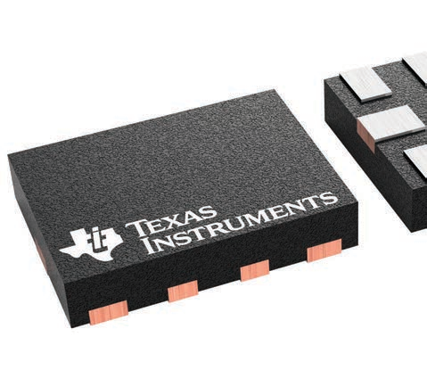
• • • • • • • • • • Solid state drive Wearables (non-medical) Professional audio amplifier (rack mount) Transimpedance Amplifier Circuit Test and measurement Motor drives Pressure transmitter Lab and field instrumentation Bridge amplifier circuit Gaming applications This op amp family is optimized for low-voltage operation as low as 2.25 V (±1.125 V) for the TLV6741 and 1.7 V (±0.85 V) for the TLV6742 and TLV6744. All of the devices operate up to 5.5 V (±2.75 V), and are specified over the temperature range of –40°C to 125°C. The single-channel TLV6741 is available in a smallsize SC70-5 package. The dual-channel TLV6742 is available in multiple package options including a tiny
100 70 50 Device Information 30 PART NUMBER (1) 20
PACKAGE BODY SIZE (NOM)
1 10 100 1k
Frequency (Hz)
10k 100k (1)
D012 For all available packages, see the orderable addendum at the end of the data sheet.
Noise Spectral Density vs Frequency An IMPORTANT NOTICE at the end of this data sheet addresses availability, warranty, changes, use in safety-critical applications, intellectual property matters and other important disclaimers. PRODUCTION DATA.
TLV6741, TLV6742 www.ti.com SBOS817I – JUNE 2017 – REVISED AUGUST 2021
1 Features............................................................................1 2 Applications..................................................................... 1 3 Description.......................................................................1 4 Revision History.............................................................. 2 5 Device Comparison Table...............................................4 6 Pin Configuration and Functions...................................5 7 Specifications.................................................................. 7
7.1 Absolute Maximum Ratings ....................................... 7 7.2 ESD Ratings .............................................................. 7 7.3 Recommended Operating Conditions ........................7 7.4 Thermal Information for Single Channel .................... 7 7.5 Thermal Information for Dual Channel .......................8 7.6 Electrical Characteristics ............................................9 7.7 TLV6741: Typical Characteristics..............................12 7.8 TLV6742: Typical Characteristics..............................18 8 Detailed Description......................................................26
8.1 Overview................................................................... 26 8.2 Functional Block Diagram......................................... 26 8.3 Feature Description...................................................26 8.4 Device Functional Modes..........................................31 9 Application and Implementation.................................. 32
9.1 Application Information............................................. 32 9.2 Single-Supply Electret Microphone Preamplifier
With Speech Filter....................................................... 32 10 Power Supply Recommendations..............................35 11 Layout........................................................................... 36
11.1 Layout Guidelines................................................... 36 11.2 Layout Example...................................................... 37 12 Device and Documentation Support..........................39
12.1 Documentation Support.......................................... 39 12.2 Receiving Notification of Documentation Updates..39 12.3 Support Resources................................................. 39 12.4 Trademarks............................................................. 39 12.5 Electrostatic Discharge Caution..............................39 12.6 Glossary..................................................................39 13 Mechanical, Packaging, and Orderable
Information.................................................................... 40
NOTE: Page numbers for previous revisions may differ from page numbers in the current version. Changes from Revision H (February 2021) to Revision I (August 2021) Page • Removed preview tag from TLV6742 VSSOP in Device Information section .................................................... 1 • Removed preview tag to VSSOP (DGK) in Device Comparison Table section.................................................. 4 Changes from Revision G (April 2020) to Revision H (February 2021) Page • Updated the numbering format for tables, figures, and cross-references throughout the document..................1 • Removed preview tag from TLV6742S X2QFN in Device Information section .................................................. 1 • Removed preview note from X2QFN for TLV6742S in Pin Configuration and Functions section...................... 5 • Removed Table of TLV6741 Graphs and Table of TLV6742 Graphs tables from the Specifications section....12 • Removed Related Links section from the Device and Documentation Support section...................................39 Changes from Revision F (January 2020) to Revision G (April 2020) Page • Added end equipment links in Application section..............................................................................................1 • Deleted preview tags for TSSOP, SOT-23, WSON, and X2QFN packages in Device Information section ....... 1 • Deleted VSSOP (8) package in Device Information section ..............................................................................1 • Added preview tag to TLV6742S X2QFN in Device Information section ........................................................... 1 • Deleted VSSOP (DGK) in Device Comparison Table section.............................................................................4 • Added preview tag to X2QFN (RUG) in Device Comparison Table section....................................................... 4 • Deleted DGK package in pinout drawing for TLV6742 package in Pin Configuration and Functions section.... 5 • Deleted DGK VSSOP in Thermal Information for Dual Channel section............................................................7 • Added shutdown electrical characteristic information........................................................................................9 • Deleted example layout for VSSOP-8 (DGK) package in Layout Example section..........................................37 Changes from Revision E (December 2019) to Revision F (January 2020) Page • Deleted TLV6744 product folder link from the data sheet page header............................................................. 1 2 Submit Document Feedback Copyright © 2021 Texas Instruments Incorporated
Product Folder Links: TLV6741 TLV6742 TLV6741, TLV6742 www.ti.com SBOS817I – JUNE 2017 – REVISED AUGUST 2021
Changes from Revision D (January 2019) to Revision E (December 2019) Page • Added I Q definition for TLV6742 and TLV744 in Features section......................................................................1 • Added EMIRR, Supply Range, I Q , and Offset Voltage Drift to Features section................................................ 1 • Changed Noise Spectral Density vs Frequency plot on front page to the TLV6742 and TLV6744 noise plot.... 1 • Changed wording of Description section to incorporate release of TLV6742 and TLV6744 devices .................1 • Changed TLV6742 packages in Device Information ..........................................................................................1 • Added Device Comparison Table section........................................................................................................... 4 • Added note regarding single supply operation to Pin Functions: TLV6741 table............................................... 5 • Added pin out drawings for TLV6742 packages in Pin Configuration and Functions section.............................5 • Added pin functions for TLV6742 packages....................................................................................................... 5 • Added X2QFN Package Drawing and Pin Functions for TLV6742S in Pin Configuration and Functions section
............................................................................................................................................................................5 • Added TLV6742 typical characteristic graphs in the Specifications section..................................................... 12 • Changed wording throughout Detailed Description section to incorporate addition of TLV6742 and TLV6744
devices..............................................................................................................................................................26 • Added EMI Rejection section with description information to Detailed Description section............................. 27 • Added Electrical Overstress section and diagram to Detailed Description section.......................................... 28 • Added Typical Specification and Distributions section to Detailed Description section.................................... 29 • Added Shutdown Function section with description for TLV6742S to Detailed Description section................. 30 • Added Packages With an Exposed Thermal Pad section to Detailed Description section...............................30 • Changed wording in Application and Implementation section to include the addition of TLV6742 and TLV6744
..........................................................................................................................................................................32 • Added TLV6742 and TLV6744 information to Power Supply Recommendations section................................ 35 • Added dual channel layout example in the Layout section...............................................................................37 Changes from Revision C (October 2017) to Revision D (January 2019) Page • Changed Operating temperature from 125 to 150 in Absolute Maximum Ratings ........................................... 7 • Added Junction temperature spec to Absolute Maximum Ratings .................................................................... 7 Changes from Revision B (October 2017) to Revision C (October 2017) Page • Added test conditions to input offset voltage parameter in Electrical Characteristics table................................ 9 • Changed typical input current noise density value from 2 fA√HZ to 23 fA√Hz................................................... 9 • Changed total supply voltage total from 5V to 5.5V in Electrical Characteristics condition statement............... 9 • Deleted "Vs = 2.25 V to 5.5 V" test conditions for common-mode rejection ratio parameter in Electrical
Characteristics ................................................................................................................................................... 9 • Deleted "C L = 0" test condition from Figure 7-25 and Figure 7-26, Figure 7-27 and Figure 7-28 ....................12 • Changed voltage step from 5 V to 2 V in Figure 7-32 ......................................................................................12 Changes from Revision A (September 2017) to Revision B (October 2017) Page • Changed Human-body model (HBM) value from: ±1000 to ±3000 and Charged-device mode (CDM) value
Changes from Revision * (June 2017) to Revision A (September 2017) Page • Changed device document status from: Advance Information to: Production Data........................................... 1 Submit Document Feedback Copyright © 2021 Texas Instruments Incorporated
Product Folder Links: TLV6741 TLV6742 3 TLV6741, TLV6742 www.ti.com SBOS817I – JUNE 2017 – REVISED AUGUST 2021
DEVICE NO. OF CHANNELS TLV6741 1
TLV6742
TLV6742S 4 2 PACKAGE LEADS
SOIC
DSC-70 DCK VSSOP DGK WSON DSG TSSOP
PW SOT-23 DDF X2QFN RUG
— 5 — — — — —
8 — 8 8 8 8 —
— — — — — — 10 Submit Document Feedback Copyright © 2021 Texas Instruments Incorporated
Product Folder Links: TLV6741 TLV6742 TLV6741, TLV6742 www.ti.com SBOS817I – JUNE 2017 – REVISED AUGUST 2021
IN+ 1
5 V+ 4 OUT Not to scale
Figure 6-1. TLV6741 DCK Package
5-Pin SC70 Top View
Table 6-1. Pin Functions: TLV6741 PIN NAME NO. IN+ 1 IN– OUT I/O DESCRIPTION I Noninverting input 3 I Inverting input 4 O Output V+ 5 — Positive (highest) supply V– 2 — Negative (lowest) supply or ground (for single-supply operation)
OUT1 1 8 V+
| PIN | I/O | DESCRIPTION | |||
|---|---|---|---|---|---|
| NAME | NO. | I/O | DESCRIPTION | ||
| IN+ | 1 | 1 | I | I | Noninverting input |
| IN– | 3 | 3 | I | I | Inverting input |
| OUT | 4 | 4 | O | O | Output |
| V+ | 5 | 5 | — | — | Positive (highest) supply |
| V– | 2 | 2 | — | — | Negative (lowest) supply or ground (for single-supply operation) |
| OUT1 1 8 V+ OUT1 1 8 V+ IN1± 2 7 OUT2 IN1± 2 7 OUT2 IN1+ 3 6 IN2± IN1+ 3 Thermal Pad 6 IN2± V± 4 5 IN2+ V± 4 5 IN2+ Not to scale Figure 6-2. TLV6742 D, DGK, PW, and DDF Package Not to scale 8-Pin SOIC, VSSOP, TSSOP, and SOT-23 Connect thermal pad to V–. See Section 8.3.8 for more Top View information. Figure 6-3. TLV6742 DSG Package 8-Pin WSON With Exposed Thermal Pad Top View Table 6-2. Pin Functions: TLV6742 | OUT1 1 8 V+ OUT1 1 8 V+ IN1± 2 7 OUT2 IN1± 2 7 OUT2 IN1+ 3 6 IN2± IN1+ 3 Thermal Pad 6 IN2± V± 4 5 IN2+ V± 4 5 IN2+ Not to scale Figure 6-2. TLV6742 D, DGK, PW, and DDF Package Not to scale 8-Pin SOIC, VSSOP, TSSOP, and SOT-23 Connect thermal pad to V–. See Section 8.3.8 for more Top View information. Figure 6-3. TLV6742 DSG Package 8-Pin WSON With Exposed Thermal Pad Top View Table 6-2. Pin Functions: TLV6742 | OUT1 1 8 V+ OUT1 1 8 V+ IN1± 2 7 OUT2 IN1± 2 7 OUT2 IN1+ 3 6 IN2± IN1+ 3 Thermal Pad 6 IN2± V± 4 5 IN2+ V± 4 5 IN2+ Not to scale Figure 6-2. TLV6742 D, DGK, PW, and DDF Package Not to scale 8-Pin SOIC, VSSOP, TSSOP, and SOT-23 Connect thermal pad to V–. See Section 8.3.8 for more Top View information. Figure 6-3. TLV6742 DSG Package 8-Pin WSON With Exposed Thermal Pad Top View Table 6-2. Pin Functions: TLV6742 | OUT1 1 8 V+ OUT1 1 8 V+ IN1± 2 7 OUT2 IN1± 2 7 OUT2 IN1+ 3 6 IN2± IN1+ 3 Thermal Pad 6 IN2± V± 4 5 IN2+ V± 4 5 IN2+ Not to scale Figure 6-2. TLV6742 D, DGK, PW, and DDF Package Not to scale 8-Pin SOIC, VSSOP, TSSOP, and SOT-23 Connect thermal pad to V–. See Section 8.3.8 for more Top View information. Figure 6-3. TLV6742 DSG Package 8-Pin WSON With Exposed Thermal Pad Top View Table 6-2. Pin Functions: TLV6742 | OUT1 1 8 V+ OUT1 1 8 V+ IN1± 2 7 OUT2 IN1± 2 7 OUT2 IN1+ 3 6 IN2± IN1+ 3 Thermal Pad 6 IN2± V± 4 5 IN2+ V± 4 5 IN2+ Not to scale Figure 6-2. TLV6742 D, DGK, PW, and DDF Package Not to scale 8-Pin SOIC, VSSOP, TSSOP, and SOT-23 Connect thermal pad to V–. See Section 8.3.8 for more Top View information. Figure 6-3. TLV6742 DSG Package 8-Pin WSON With Exposed Thermal Pad Top View Table 6-2. Pin Functions: TLV6742 | OUT1 1 8 V+ OUT1 1 8 V+ IN1± 2 7 OUT2 IN1± 2 7 OUT2 IN1+ 3 6 IN2± IN1+ 3 Thermal Pad 6 IN2± V± 4 5 IN2+ V± 4 5 IN2+ Not to scale Figure 6-2. TLV6742 D, DGK, PW, and DDF Package Not to scale 8-Pin SOIC, VSSOP, TSSOP, and SOT-23 Connect thermal pad to V–. See Section 8.3.8 for more Top View information. Figure 6-3. TLV6742 DSG Package 8-Pin WSON With Exposed Thermal Pad Top View Table 6-2. Pin Functions: TLV6742 |
| PIN | PIN | PIN | PIN | I/O | DESCRIPTION |
| NAME | NAME | NO. | NO. | I/O | DESCRIPTION |
| IN1– | IN1– | 2 | 2 | I | Inverting input, channel 1 |
| IN1+ | IN1+ | 3 | 3 | I | Noninverting input, channel 1 |
| IN2– | IN2– | 6 | 6 | I | Inverting input, channel 2 |
| IN2+ | IN2+ | 5 | 5 | I | Noninverting input, channel 2 |
| OUT1 | OUT1 | 1 | 1 | O | Output, channel 1 |
| OUT2 | OUT2 | 7 | 7 | O | Output, channel 2 |
Product Folder Links: TLV6741 TLV6742 5
www.ti.com SBOS817I – JUNE 2017 – REVISED AUGUST 2021
PIN NAME I/O NO.
DESCRIPTION 4 — Negative (lowest) supply or ground (for single-supply operation) V+ 8 — Positive (highest) supply IN1+ V–
| PIN | I/O | DESCRIPTION | ||||
|---|---|---|---|---|---|---|
| NAME | NO. | I/O | DESCRIPTION | |||
| V– | V– | 4 | 4 | — | — | Negative (lowest) supply or ground (for single-supply operation) |
| V+ | V+ | 8 | 8 | — | — | Positive (highest) supply |
| IN1+ V± 1 9 IN1± 10 SHDN1 2 8 OUT1 SHDN2 3 7 V+ 5 IN2+ 4 6 OUT2 Not to scale IN2± Figure 6-4. TLV6742S RUG Package 10-Pin X2QFN Top View Table 6-3. Pin Functions: TLV6742S | IN1+ V± 1 9 IN1± 10 SHDN1 2 8 OUT1 SHDN2 3 7 V+ 5 IN2+ 4 6 OUT2 Not to scale IN2± Figure 6-4. TLV6742S RUG Package 10-Pin X2QFN Top View Table 6-3. Pin Functions: TLV6742S | IN1+ V± 1 9 IN1± 10 SHDN1 2 8 OUT1 SHDN2 3 7 V+ 5 IN2+ 4 6 OUT2 Not to scale IN2± Figure 6-4. TLV6742S RUG Package 10-Pin X2QFN Top View Table 6-3. Pin Functions: TLV6742S | IN1+ V± 1 9 IN1± 10 SHDN1 2 8 OUT1 SHDN2 3 7 V+ 5 IN2+ 4 6 OUT2 Not to scale IN2± Figure 6-4. TLV6742S RUG Package 10-Pin X2QFN Top View Table 6-3. Pin Functions: TLV6742S | IN1+ V± 1 9 IN1± 10 SHDN1 2 8 OUT1 SHDN2 3 7 V+ 5 IN2+ 4 6 OUT2 Not to scale IN2± Figure 6-4. TLV6742S RUG Package 10-Pin X2QFN Top View Table 6-3. Pin Functions: TLV6742S | IN1+ V± 1 9 IN1± 10 SHDN1 2 8 OUT1 SHDN2 3 7 V+ 5 IN2+ 4 6 OUT2 Not to scale IN2± Figure 6-4. TLV6742S RUG Package 10-Pin X2QFN Top View Table 6-3. Pin Functions: TLV6742S | IN1+ V± 1 9 IN1± 10 SHDN1 2 8 OUT1 SHDN2 3 7 V+ 5 IN2+ 4 6 OUT2 Not to scale IN2± Figure 6-4. TLV6742S RUG Package 10-Pin X2QFN Top View Table 6-3. Pin Functions: TLV6742S |
| PIN | PIN | PIN | I/O | I/O | DESCRIPTION | DESCRIPTION |
| NAME | NO. | NO. | I/O | I/O | DESCRIPTION | DESCRIPTION |
| IN1– | 9 | 9 | I | I | Inverting input, channel 1 | Inverting input, channel 1 |
| IN1+ | 10 | 10 | I | I | Noninverting input, channel 1 | Noninverting input, channel 1 |
| IN2– | 5 | 5 | I | I | Inverting input, channel 2 | Inverting input, channel 2 |
| IN2+ | 4 | 4 | I | I | Noninverting input, channel 2 | Noninverting input, channel 2 |
| OUT1 | 8 | 8 | O | O | Output, channel 1 | Output, channel 1 |
| OUT2 | 6 | 6 | O | O | Output, channel 2 | Output, channel 2 |
| SHDN1 | 2 | 2 | I | I | Shutdown: low = amp disabled, high = amp enabled. Channel 1. See Section 8.3.7 for more information. | Shutdown: low = amp disabled, high = amp enabled. Channel 1. See Section 8.3.7 for more information. |
| SHDN2 | 3 | 3 | I | I | Shutdown: low = amp disabled, high = amp enabled. Channel 2. See Section 8.3.7 for more information. | Shutdown: low = amp disabled, high = amp enabled. Channel 2. See Section 8.3.7 for more information. |
| V– | 1 | 1 | I or — | I or — | Negative (lowest) supply or ground (for single-supply operation) | Negative (lowest) supply or ground (for single-supply operation) |
| V+ | 7 | 7 | I | I | Positive (highest) supply | Positive (highest) supply |
Product Folder Links: TLV6741 TLV6742
www.ti.com SBOS817I – JUNE 2017 – REVISED AUGUST 2021
MIN MAX
0 6 V (V–) – 0.5 (V+) + 0.5 V
Common-mode voltage (3) Differential voltage (3) (4) Signal input pins
Current (3)
V S + 0.2 V
10 mA 150 °C 150 °C 150 °C –10 Output short-circuit (2) Continuous Operating ambient temperature, T A –55 Junction temperature, T J Storage temperature, T stg
(1)
(2) (3)
(4)
UNIT –65
Operating the device beyond the ratings listed under Absolute Maximum Ratings will cause permanent damage to the device. These are stress ratings only, based on process and design limitations, and this device has not been designed to function outside the conditions indicated under Recommended Operating Conditions. Exposure to any condition outside Recommended Operating Conditions for extended periods, including absolute-maximum-rated conditions, may affect device reliability and performance. Short-circuit to ground, one amplifier per package. Input pins are diode-clamped to the power-supply rails. Input signals that may swing more than 0.5 V beyond the supply rails must be current limited to 10 mA or less. Differential input voltages greater than 0.25 V applied continuously can result in a shift to the input offset voltage above the maximum specification of this parameter. The magnitude of this effect increases as the ambient operating temperature rises.
VALUE V (ESD) Electrostatic discharge TLV6741: Human-body model (HBM), per ANSI/ESDA/JEDEC JS-001 (1) ±3000 TLV6742: Human-body model (HBM), per ANSI/ESDA/JEDEC JS-001 (1) ±2000 All Devices: Charged-device model (CDM), per JEDEC specification JESD22-C101 (2)
(1) (2)
UNIT V ±1500 JEDEC document JEP155 states that 500-V HBM allows safe manufacturing with a standard ESD control process. JEDEC document JEP157 states that 250-V CDM allows safe manufacturing with a standard ESD control process.
MIN MAX UNIT V S Supply voltage, (V+) – (V–) , for TLV6742 and TLV6744 1.7 (1) 5.5 V V S Supply voltage, (V+) – (V–), for TLV6741 only 2.25 5.5 V V I Input voltage range (V–) (V+) – 1.2 V T A Specified temperature –40 125 °C
(1) Operation between 1.7V and 1.8V is only recommened for T A = 0 - 85 ℃
TLV6741 THERMAL METRIC (1) DCK (SC70) UNIT
5 PINS R θJA Junction-to-ambient thermal resistance 240.9 ℃/W R θJC(top) Junction-to-case (top) thermal resistance 151.7 ℃/W R θJB Junction-to-board thermal resistance 64 ℃/W ψ JT Junction-to-top characterization parameter 34.8 ℃/W ψ JB Junction-to-board characterization parameter 63.3 ℃/W Submit Document Feedback Copyright © 2021 Texas Instruments Incorporated
Product Folder Links: TLV6741 TLV6742 7
www.ti.com SBOS817I – JUNE 2017 – REVISED AUGUST 2021
TLV6741
DCK (SC70) THERMAL METRIC
(1) UNIT 5 PINS R θJC(bot)
(1)
Junction-to-case (bottom) thermal resistance ℃/W n/a
For more information about traditional and new thermal metrics, see the Semiconductor and IC Package Thermal Metrics application report SPRA953C.
TLV6742, TLV6742S THERMAL METRIC (1) D (SOIC) DDF (SOT-23-8) DSG (WSON) PW (TSSOP) DGK (VSSOP) RUG (X2QFN) UNIT
8 PINS 8 PINS 8 PINS 8 PINS 8 PINS 10 PINS R θJA Junction-to-ambient thermal resistance 131.1 153.8 78.2 185.6 177.0 140.3 °C/W R θJC(top) Junction-to-case (top) thermal resistance 73.2 80.2 97.5 74.5 68.6 52.6 °C/W R θJB Junction-to-board thermal resistance 74.5 73.1 44.6 116.3 98.7 69.7 °C/W ψ JT Junction-to-top characterization parameter 24.4 6.6 4.7 12.6 12.4 1.0 °C/W ψ JB Junction-to-board characterization parameter 73.3 72.7 44.6 114.6 97.1 67.5 °C/W R θJC(bot) Junction-to-case (bottom) thermal resistance n/a n/a 19.8 n/a n/a n/a °C/W
(1) For more information about traditional and new thermal metrics, see the Semiconductor and IC Package Thermal Metrics application
report, SPRA953C.
8 Submit Document Feedback Copyright © 2021 Texas Instruments Incorporated
Product Folder Links: TLV6741 TLV6742
www.ti.com SBOS817I – JUNE 2017 – REVISED AUGUST 2021
PARAMETER TEST CONDITIONS MIN TYP MAX
UNIT OFFSET VOLTAGE
mV µV/℃ μV/V dB INPUT BIAS CURRENT I B Input bias current I OS Input offset current
pA pA NOISE E N Input voltage noise f = 0.1 to 10 Hz f = 10 Hz e N Input voltage noise density
i N Input current noise 1.2 μV PP 0.227 µV RMS TLV6742/4 (3) 30 TLV6741 (2) 5.0 TLV6742/4 (3) 4.6 TLV6741 (2) 3.7 TLV6742/4 (3) 3.5 nV/√Hz
INPUT VOLTAGE RANGE V CM Common-mode voltage range CMRR Common-mode rejection ratio (V–)
TLV6741 (2)
TLV6742/4 (3)
(V+) -1.2 95 120 87 100 94 110 V dB INPUT CAPACITANCE Z ID Differential 10 || 6 MΩ || pF Z ICM Common-mode 10 || 6 GΩ || pF OPEN-LOOP GAIN
125 TLV6741 (2)
110 130 107 120
dB 140
110 120 140 Submit Document Feedback Copyright © 2021 Texas Instruments Incorporated
Product Folder Links: TLV6741 TLV6742 9
www.ti.com SBOS817I – JUNE 2017 – REVISED AUGUST 2021
PARAMETER TEST CONDITIONS MIN TYP MAX UNIT FREQUENCY RESPONSE GBW Gain-bandwidth product SR Slew rate t S Settling time
Phase margin G = +1, R L = 10kΩ, C L = 20 pF 55 ° Overload recovery time V IN × gain > V S 0.2 μs
THD+N Total harmonic distortion + noise V S = 5.5 V, V CM = 2.5 V, V O = 1 V RMS , G = +1, f = 1 kHz, R
L = 10 kΩ TLV6741 (2) 0.00035% TLV6742/4 (3) 0.00015% EMIRR Electro-magnetic interference rejection ratio
dB OUTPUT
Positive/Negative rail headroom Voltage output swing from rail Positive rail headroom
Capacitive load drive Z O Open-loop output impedance 5 TLV6742/4 (3) Short-circuit current C LOAD
I SC 14
See Figure
Ω POWER SUPPLY I Q Quiescent current per amplifier V S = 5.5 V, I O = 0 A
Turn-On Time 10 At T A = 25°C, V S = 5.5 V, V S ramp rate > 0.3 V/µs TLV6741 (2)
TLV6742/4 (3)
TLV6742/4 (3)
Submit Document Feedback 890
1100 990 1200 µA 1250 10 μs Copyright © 2021 Texas Instruments Incorporated
Product Folder Links: TLV6741 TLV6742
www.ti.com SBOS817I – JUNE 2017 – REVISED AUGUST 2021
| PARAMETER | TEST CONDITIONS | MIN TYP MAX | UNIT | ||||||
|---|---|---|---|---|---|---|---|---|---|
| SHUTDOWN | |||||||||
| IQSD | Quiescent current per amplifier | All amplifiers disabled, SHDN = V– | 1 3.5 | µA | |||||
| ZSHDN | Output impedance during shutdown | Amplifier disabled | 10 \ | \ | 6 | GΩ \ | \ | pF | |
| VIH | Logic high threshold voltage (amplifier enabled) | (V–) + 1.1 V | V | ||||||
| VIL | Logic low threshold voltage (amplifier disabled) | (V–) + 0.2V | V | ||||||
| tON | Amplifier enable time (full shutdown)(1) | G = +1, VCM = V-, VO = 0.1 × VS /2 | 15 | µs | |||||
| tON | Amplifier enable time (partial shutdown)(1) | G = +1, VCM = V-, VO = 0.1 × VS /2 | 8 | µs | |||||
| tOFF | Amplifier disable time(1) | VCM = V-, VO = VS /2 | 3 | µs | |||||
| SHDN pin input bias current (per pin) | (V+) ≥ SHDN ≥ (V–) + 0.9 V | 0.4 | µA | ||||||
| SHDN pin input bias current (per pin) | (V–) ≤ SHDN ≤ (V–) + 0.7 V | 0.25 | µA | ||||||
t ON t OFF (2) (3)
GΩ || pF (V–) + 1.1
V
V(V–) + 0.2
V
Amplifier disable time (1) V CM = V-, V O = V S /2
SHDN pin input bias current (per pin)
(1)
10 || 6 µs
µA Disable time (t OFF ) and enable time (t ON ) are defined as the time interval between the 50% point of the signal applied to the SHDN pin and the point at which the output voltage reaches the 10% (disable) or 90% (enable) level. This electrical characteristic only applies to the single-channel, TLV6741 This electrical characteristic only applies to the dual-channel TLV6742 and quad-channel TLV6744 Submit Document Feedback Copyright © 2021 Texas Instruments Incorporated
Product Folder Links: TLV6741 TLV6742 11
www.ti.com SBOS817I – JUNE 2017 – REVISED AUGUST 2021
80 35% 70 30% 60 Population (%)
40% 25% 20% 15% 50 40 30
10% 20 5% 10
0 0
-1000 -900 -800 -700 -600 -500 -400 -300 -200 -100 0 100 200 300 400 500 600 700 800 900 1000 Population (%)
0.4 6 100 4 -100 -200 -300 -400
-60 1.2 1.6 2 2.4 2.8
D002 Figure 7-2. Offset Voltage Drift Distribution
200 0 0.8
Offset Voltage Drift (PV/qC)
Offset Voltage (mV)
Offset Voltage (PV)
D001 Offset Voltage (µV) Figure 7-1. Offset Voltage Production Distribution 2 0 -2 -4 -6 -40 -20 0 20 40 60 80
Temperature (qC)
100 120 140 -4 -3
D003 Figure 7-3. Offset Voltage vs Temperature -2 -1 0 1 2 Input Common Mode Voltage (V)
3 4
D004 Figure 7-4. Offset Voltage vs Common-Mode Voltage
0.5 300
0.4 200 100 0.2
0.1 V OS (PV)
Offset Voltage (mV)
0.3 0
-0.1 -100 -200 -0.2
-300 -0.3 -400 -0.4
-0.5
-2.5 -2 -1.5 -1 -0.5 0 0.5 1
Input Common Mode Voltage (V)
1.5 Figure 7-5. Offset Voltage vs Common-Mode Voltage 12 0 2 -500
1.5
D004 2.5 3.5
V S (V)
4.5 5.5
D005 Figure 7-6. Offset Voltage vs Power Supply Submit Document Feedback Copyright © 2021 Texas Instruments Incorporated
Product Folder Links: TLV6741 TLV6742
www.ti.com SBOS817I – JUNE 2017 – REVISED AUGUST 2021
8 20
I B I B + I OS 6 4 -20 I B and I OS (pA)
IB and I OS (pA)
I B I B I OS 0 2 0 -2 -40 -60 -80 -4
-100 -6 -8 -120
-4 -3 -2 -1 0 1 2 3
V CM (V)
4 0 100 100 40 75 75 30 50 50 25 25 0 0 -25 -25 Gain Phase -75
1k 10k 100k 1M
Frequency (Hz)
100 Temperature (qC)
150
D044 Figure 7-8. I B and I OS vs Temperature Gain (dB)
20 Phase (q)
Open-Loop Gain (dB)
Figure 7-7. I B and I OS vs Common-Mode Voltage -50 50
D043 10 0 -10 -20
-50 -30 -75 -40 1k 10M 10k 100k
Frequency (Hz) D006 1M 10M
D007 Figure 7-10. Closed-Loop Gain vs Frequency C L = 10 pF Figure 7-9. Open-Loop Gain and Phase vs Frequency
120 3
PSRR (dB) PSRR+ (dB) 2.5
100 2
-40 ° C 125°C 1 85 ° C 25 ° C 80 PSRR (dB)
Output Voltage (V)
1.5 0.5
0 -0.5 60 40 -1 125 ° C -1.5 85 ° C 25 ° C -40 ° C
20 -2 -2.5
-3 10 15 20 25 30 35 40 45
Output Current (mA)
50 55 60 0 1k Figure 7-11. V O vs I Sourcing and Sinking 10k 100k
Frequency (Hz) D010 1M
D011 Figure 7-12. PSRR vs Frequency (Referred to Input)
Submit Document Feedback Copyright © 2021 Texas Instruments Incorporated
Product Folder Links: TLV6741 TLV6742 13
www.ti.com SBOS817I – JUNE 2017 – REVISED AUGUST 2021
120 10 110 100 90 5 CMRR (PV/V) CMRR (dB)
80 70 60 50 40 0 30 -5 20 10 0 1k 10k 100k -10 -50 1M Frequency (Hz)
0
D011 Figure 7-13. CMRR vs Frequency (Referred to Input)
50 Temperature (qC)
100 150
D012
Figure 7-14. CMRR vs Temperature Voltage (0.5PV/div)
Input Voltage Noise Spectral Density (nV/—Hz)
100 1 10 Time (1 s/div)
D014 -95 -95 -97 -97 -99 -101 -103 -105
100 100 1k
Frequency (Hz)
10k 100k
D015 Figure 7-16. Input Voltage Noise Spectral Density vs Frequency THD + N (dB)
THD + N (dB)
Figure 7-15. 0.1-Hz to 10-Hz Flicker Noise 14 10 -99 -101 -103 1k Frequency (Hz)
-105 100 10k 1k
Frequency (Hz) D017
Gain = 1, BW = 80 kHz, V OUT = 0.5 Vrms
Gain = 1, BW = 80 kHz, V OUT = 0.5 Vrms Figure 7-17. THD + N vs Frequency Figure 7-18. THD + N vs Frequency Submit Document Feedback D017 Copyright © 2021 Texas Instruments Incorporated
Product Folder Links: TLV6741 TLV6742
www.ti.com SBOS817I – JUNE 2017 – REVISED AUGUST 2021
1000 0
-40 -60 -80 -100 850
800
750
700
650
600
550 -120
0.001 0.01 0.1
V OUT (rms)
1 5 500
1.5 D018
BW = 80 kHz, V OUT = 0.5 Vrms 2 2.5 3 3.5 4
Supply Voltage (V)
4.5 5 5.5
D020 Figure 7-20. Quiescent Current vs Supply Voltage
Figure 7-19. THD + N vs Amplitude 9
900 8 Open-Loop Gain (PV/V)
10
950 Quiescent Current (PA)
1000 850
800
750
700
650
600 A VDD = 5.5 V A VDD = 1.8 V 7
6
5
4
3
2
550 1
500
-50 0 -60 0 50
Temperature (qC)
100 150 -40 -20 0
D021 Figure 7-21. Quiescent Current vs Temperature 20 40 60 80 Temperature (qC)
100 120 140
D022 R L = 2 kΩ Figure 7-22. Open-Loop Gain vs Temperature
1000 160 Open-Loop Impedance (:)
Open Loop Voltage Gain (dB)
200 120 80 40 0
0 0.5 1 1.5 2 2.5 3 3.5 4 4.5
Output Voltage (V)
5 5.5 100 10
1k 10k
C023 Figure 7-23. Open-Loop Gain vs Output Voltage 100k Frequency (Hz)
1M 10M
D024 A VDD = 5.5 V, V ICM = V OCM = 2.75 V Figure 7-24. Open-Loop Output Impedance vs Frequency Submit Document Feedback Copyright © 2021 Texas Instruments Incorporated
Product Folder Links: TLV6741 TLV6742 15
TLV6741, TLV6742 www.ti.com SBOS817I – JUNE 2017 – REVISED AUGUST 2021
50 50 40 40 Overshoot (%) Overshoot (%)
at T A = 25°C, V S = 5.5 V, R L = 10 kΩ connected to V S / 2, V CM = V S / 2, and V OUT = V S / 2, unless otherwise noted.
30 20 10 30 20 10 Overshoot (+) Overshoot ( )
Overshoot (+) Overshoot ( ) 0 0 0 10 20 30 40 50 60 70
Capacitive Load (pF)
80 90 100 0 10
V OCM = 2.75 V, G = 1, 100-mV output step 30 40 50 60
Capacitance (pF)
70 80 90 100
D025
V OCM = 0.9 V, G = 1, 100-mV output step Figure 7-25. Small-Signal Overshoot vs Load Capacitance Figure 7-26. Small-Signal Overshoot vs Load Capacitance
50 50 40 40 Overshoot (%) Overshoot (%)
20
D025 30 20 10 30 20 10 Overshoot (+) Overshoot ( )
Overshoot (+) Overshoot ( ) 0 0 0 10 20 30 40 50 60 70
Capacitive Load (pF)
80 90 100 0 10 20
D025
V OCM = 2.75 V, Gain = –1, 100-mV output step 30 40 50 60
Capacitance (pF)
70 80 90 100
D025
V OCM = 0.9 V, Gain = –1, 100-mV output step Figure 7-27. Small-Signal Overshoot vs Load Capacitance Figure 7-28. Small-Signal Overshoot vs Load Capacitance Voltage (1 V/div)
Voltage (1 V/div)
Input Output Input Output Time (2 Ps/div) Time (25 Ps/div)
D027 Figure 7-29. No Phase Reversal 16 D028 Figure 7-30. Overload Recovery Submit Document Feedback Copyright © 2021 Texas Instruments Incorporated
Product Folder Links: TLV6741 TLV6742 TLV6741, TLV6742 www.ti.com SBOS817I – JUNE 2017 – REVISED AUGUST 2021
at T A = 25°C, V S = 5.5 V, R L = 10 kΩ connected to V S / 2, V CM = V S / 2, and V OUT = V S / 2, unless otherwise noted.
V IN V OUT Voltage (0.5 V/div)
Voltage (20 mV/div)
V IN V OUT Time (1 Ps/div) Time (2 Ps/div)
D030 D031
V ICM = 2.75 V, Gain = 1, 2-V step Figure 7-31. Small-Signal Step Response Figure 7-32. Large Signal Step Response Output Voltage ( 5 mV/div)
Output Voltage (10 mV/div)
V S = 1.8 V, V ICM = 0.9 V, V OCM = 0.9 V
Time (0.2 Ps/div) Time (0.1 Ps/div)
D032 D033 V S = 5.5 V, V ICM = 2.75 V, V OCM = 2.75 V
C L = 0, Gain = 1, 5-V step V S = 5.5 V, V ICM = 2.75 V, V OCM = 2.75 V
C L = 0, Gain = 1, 5-V step Figure 7-33. Large Signal Settling Time (Positive) Figure 7-34. Large Signal Settling Time (Negative)
100 6
Sourcing Sinking Maximum Output Voltage (V)
Short Circuit Current (mA)
80
60
40
20
0
-20
-40
-60 V S = 1.8 V V S = 5.5 V 5 4 3 2 1 -80
-100
-50 0 0 50
Temperature (qC)
100 150 1 10
D034 Figure 7-35. Short-Circuit Current vs Temperature 100 1k 10k 100k
Frequency (Hz)
1M 10M 100M
D035 V ICM = V S / 2, V OCM = V S / 2,
Figure 7-36. Maximum Output Voltage vs Frequency Submit Document Feedback Copyright © 2021 Texas Instruments Incorporated
Product Folder Links: TLV6741 TLV6742 17 TLV6741, TLV6742 www.ti.com SBOS817I – JUNE 2017 – REVISED AUGUST 2021
at T A = 25°C, V S = 5.5 V, R L = 10 kΩ connected to V S / 2, V CM = V S / 2, and V OUT = V S / 2, unless otherwise noted.
120 60 50 Phase Margin (q)
EMIRR IN + (dB)
100 80 60 40 20 10M 40 30 20 10
V S = 1.8 V V S = 5.5 V 0 100M 1G
Frequency (Hz)
10G 0 20 40 Capacitive Load (pF) D036 Figure 7-37. Electromagnetic Interference Rejection Ratio Referred to Noninverting Input (EMIRR+) vs Frequency 60
D037 V ICM = V OCM = V S / 2 Figure 7-38. Phase Margin vs Capacitive Load
2500 22 2250 20 2000 18 16 1750 Population (%)
Number of Amplifiers (#)
at T A = 25°C, V S = ±2.75 V, R L = 10 kΩ connected to V S / 2, V CM = V S / 2, and V OUT = V S / 2, unless otherwise noted.
1500
1250
1000 14 12 10 8 750 6 500 4 250 2
0 -500 -400 -300 -200 -100 0 100 200 300 400 500
Offset Voltage (µV) D001
V CM = V– 0
0 0.05 0.1 0.15 0.2 0.25 0.3 0.35 0.4 0.45 0.5
Offset Voltage Drift (PV/qC) D002 Figure 7-40. Offset Voltage Drift Distribution Figure 7-39. Offset Voltage Production Distribution 18 Submit Document Feedback Copyright © 2021 Texas Instruments Incorporated
Product Folder Links: TLV6741 TLV6742 TLV6741, TLV6742 www.ti.com SBOS817I – JUNE 2017 – REVISED AUGUST 2021
200 4800 160 4000 120 3200 Offset Voltage (µV)
Offset Voltage (µV)
at T A = 25°C, V S = ±2.75 V, R L = 10 kΩ connected to V S / 2, V CM = V S / 2, and V OUT = V S / 2, unless otherwise noted.
80
40
0
-40
-80 2400 1600 800
0 -800 -1600 -120 -2400 -160 -3200 -200
-40 -20 0 20 40 60 80
Temperature (qC)
100 120 -4000 -40 140 -20 0 20
D003 V CM = V– 120 140
D004 Figure 7-42. Offset Voltage vs Temperature (NMOS Input Pair)
5000 200
4000 160 3000 120 Offset Voltage (µV)
Offset Voltage (µV)
100 V CM = V+ Figure 7-41. Offset Voltage vs Temperature (PMOS Input Pair)
2000
1000
0
-1000 80
40
0
-40
-80 -2000 -120 -3000 -160
-4000
-3 40 60 80 Temperature (°C)
-2.4 -1.8 -1.2 -0.6 0 0.6 1.2 1.8
Input Common Mode Voltage (V)
2.4 -200 -3 3 -2.5 -2
D005 Over full common-mode voltage range Figure 7-43. Offset Voltage vs Common-Mode Voltage (Full
Range)
-1.5 -1 -0.5 0 0.5 1 Input Common Mode Voltage (V)
1.5 2
D006 Figure 7-44. Offset Voltage vs Common-Mode Voltage (PMOS
Input Pair)
300 4000
240
180 2000 Offset Voltage (PV)
Offset Voltage (µV)
3000 1000 0
-1000
-2000 120
60
0
-60
-120
-180 -3000
-4000
1.8 -240 1.9 2 2.1 2.2
Input Common Mode Voltage (V)
2.3 Figure 7-45. Offset Voltage vs Common-Mode Voltage
(Transition Region)
2.4 -300
1.5 2 D007 2.5 3 3.5 4 4.5
Supply Voltage (V)
5 5.5 6
D008 Figure 7-46. Offset Voltage vs Power Supply Submit Document Feedback Copyright © 2021 Texas Instruments Incorporated
Product Folder Links: TLV6741 TLV6742 19 TLV6741, TLV6742 www.ti.com SBOS817I – JUNE 2017 – REVISED AUGUST 2021
at T A = 25°C, V S = ±2.75 V, R L = 10 kΩ connected to V S / 2, V CM = V S / 2, and V OUT = V S / 2, unless otherwise noted.
320
40 280 30 240 I B and I OS current (pA)
50 I B and I OS (pA)
20
10
0
-10
-20
-30 I
BI B+ I OS -40
-50
-3 -2.5 -2 -1.5 -1 -0.5 0 0.5
V CM (V)
1 1.5 2 2.5 I BI B+ I OS 200
160
120
80
40
0
-40 -40 3 -20 0 20
D009 120 140
D010 Voltage (0.2 PV/div)
100 70 50
30 20 10 7 5
3 2 1 10 Time (1 s/div) 100 1k
Frequency (Hz) D011 Figure 7-49. 0.1-Hz to 10-Hz Flicker Noise 10k 100k
D012 Figure 7-50. Input Voltage Noise Spectral Density vs Frequency
120 130
CMRR PSRR+ PSRR- 110
115 90 CMRR (dB)
PSRR and CMRR (dB)
100 Figure 7-48. I B and I OS vs Temperature Voltage noise spectral density (nV/rtHz)
Figure 7-47. I B and I OS vs Common-Mode Voltage 40 60 80 Temperature (°C)
70 110 50
105 30 10
1k 10k 100k
Frequency (Hz)
1M 10M 100
-40 -20 0
D013 Figure 7-51. CMRR and PSRR vs Frequency (Referred to Input)
20 40 60 80
Temperature (°C)
100 120 140
D014
Figure 7-52. CMRR vs Temperature 20 Submit Document Feedback Copyright © 2021 Texas Instruments Incorporated
Product Folder Links: TLV6741 TLV6742
TLV6741, TLV6742 www.ti.com SBOS817I – JUNE 2017 – REVISED AUGUST 2021
120 130 Gain (dB) PSRR (dB)
125 120 115 110
-40 -20 0 20 40 60 80
Temperature (°C)
100 120 140 100 210 Gain Phase 180 80 150 60 120 40 90 20 60 0 30 -20
100 0 1k 10k 100k Frequency (Hz) D015 V CM = V– 60 0.6 Open Loop Voltage Gain (uV/V)
0.66 Gain (dB)
40 20 0 -20
-80
1k 10M
D016 Figure 7-54. Open-Loop Gain and Phase vs Frequency
80 -60 1M C L = 10 pF Figure 7-53. PSRR vs Temperature -40 Phase (degree)
at T A = 25°C, V S = ±2.75 V, R L = 10 kΩ connected to V S / 2, V CM = V S / 2, and V OUT = V S / 2, unless otherwise noted.
0.54
0.48
0.42
0.36
0.3
0.24
0.18
0.12 10k 100k
Frequency (Hz)
1M 0.06 -40 10M -20 0
D017 20 40 60 80
Temperature (°C)
100 120 140
D018 Figure 7-56. Open-Loop Gain vs Temperature C L = 10 pF Figure 7-55. Closed-Loop Gain vs Frequency
180 55
160
50
120 Phase Margin (°)
Open-Loop Gain (dB)
140 100
80
60
40
20 45 40 35
0
-20
-0.5 0.5 1.5 2.5 3.5
Output Voltage (V)
4.5 30 10 5.5 20
D019 Figure 7-57. Open-Loop Gain vs Output Voltage 30 40 50 60 70
Capacitive Load (pF)
80 90 100
D020 Figure 7-58. Phase Margin vs Capacitive Load Submit Document Feedback Copyright © 2021 Texas Instruments Incorporated
Product Folder Links: TLV6741 TLV6742 21 TLV6741, TLV6742 www.ti.com SBOS817I – JUNE 2017 – REVISED AUGUST 2021
at T A = 25°C, V S = ±2.75 V, R L = 10 kΩ connected to V S / 2, V CM = V S / 2, and V OUT = V S / 2, unless otherwise noted.
4 60
Input Output 3
50 Overshoot (%) Amplitude (V)
2 1 0 -1 40 30 20 -2
10 -3 -4 0
0 Time (10 µs/div) 20
D021 Figure 7-59. No Phase Reversal 40 60 Capacitive Load (pF)
80 100
D022
Gain = –1, 100-mV output step Figure 7-60. Small-Signal Overshoot vs Load Capacitance
5 70
R ISO = 0:, Overshoot (-)
R ISO = 50:, Overshoot (-)
60
2.5 Amplitude (V) Overshoot (%)
50 40 30 20 0 -2.5
10 Input
Output -5 0 0 25 50 75
Capacitive Load (pF)
100 Time (10 µs/div) 125
D024 D023
Gain = +1, 100-mV output step
Figure 7-62. Overload Recovery Figure 7-61. Small-Signal Overshoot vs Load Capacitance 22 Submit Document Feedback Copyright © 2021 Texas Instruments Incorporated
Product Folder Links: TLV6741 TLV6742 TLV6741, TLV6742 www.ti.com SBOS817I – JUNE 2017 – REVISED AUGUST 2021
at T A = 25°C, V S = ±2.75 V, R L = 10 kΩ connected to V S / 2, V CM = V S / 2, and V OUT = V S / 2, unless otherwise noted.
0.1 0.1
Input Output Input Output 0.08 0.06 0.06
0.04 0.04 Amplitude (V) Amplitude (V)
0.08 0.02
0
-0.02 0.02
0
-0.02
-0.04 -0.04
-0.06 -0.06
-0.08 -0.08
-0.1 -0.1
Time (1 µs/div) Time (1 µs/div)
D027 D025 C L = 20 pF, Gain = 1, V IN = 100-mVpp , R L = 1 kΩ C L = 20 pF, Gain = –1, V IN = 100-mVpp, R L = 1 kΩ Figure 7-63. Small-Signal Step Response Figure 7-64. Small-Signal Step Response
1.25 1.25
Input Output Input Output 1 0.75 0.75
0.5 0.5 Amplitude (V) Amplitude (V)
1 0.25
0
-0.25 0.25
0
-0.25
-0.5 -0.5
-0.75 -0.75
-1 -1
-1.25 -1.25
Time (1 µs/div) Time (1 µs/div)
D026 D028 Figure 7-65. Large Signal Step Response Figure 7-66. Large Signal Step Response Output Delta from Final Value (5 mV/div)
Output Delta from Final Value (5 mV/div)
0.1% Settling Time Step Applied at t = 0 0.1% Settling Time Step Applied at t = 0 Time (0.25 Ps/div) Time (0.25 Ps/div)
D029 C L = 20 pF, Gain = 1, V IN = 2-V step Figure 7-67. Large Signal Settling Time (Positive)
D050 C L = 20 pF, Gain = –1, V IN = 2-V step Figure 7-68. Large Signal Settling Time (Negative)
Submit Document Feedback Copyright © 2021 Texas Instruments Incorporated
Product Folder Links: TLV6741 TLV6742 23 TLV6741, TLV6742 www.ti.com SBOS817I – JUNE 2017 – REVISED AUGUST 2021
at T A = 25°C, V S = ±2.75 V, R L = 10 kΩ connected to V S / 2, V CM = V S / 2, and V OUT = V S / 2, unless otherwise noted.
THD+N
-104
Gain = +1, BW = 80 kHz, V OUT = 0.5 Vrms 3 2.8 2.6 2.4 2.2
2 1.8 1.6 1.4 1.2
1 0.8 0.6 0.4 0.2
0 -40q 25q 85q 125q Output Voltage (V)
Output Voltage (V)
D031 Figure 7-70. THD + N vs Amplitude
0 -0.2 -0.4 -0.6 -0.8
-1 -1.2 -1.4 -1.6 -1.8
-2 -2.2 -2.4 -2.6 -2.8
-3 5 10 15 20 25 30 35 40 45 50 55 60 65 70 75 80
Output Current (mA) D032 -40q 25q 85q 125q 0 Figure 7-71. V OUT vs Sourcing Current 5 10 15 20 25 30 35 40 45 50 55 60 65 70 75 80
Output Current (mA) D033 Figure 7-72. V OUT vs Sinking Current
6 80 Short Circuit Current Limit (mA)
Maximum Output Voltage (V)
1
Figure 7-69. THD + N vs Frequency 0 5 4 3 2 1 0 1 10 100 1k 10k 100k
Frequency (Hz)
1M 10M 100M 75 70 65 60 55 50
-40 -20
D034
0 20 40 60 80
Temperature (°C)
100 120 140
D035 Figure 7-74. Short-Circuit Current vs Temperature
Figure 7-73. Maximum Output Voltage vs Frequency 24 Submit Document Feedback Copyright © 2021 Texas Instruments Incorporated
Product Folder Links: TLV6741 TLV6742 TLV6741, TLV6742 www.ti.com SBOS817I – JUNE 2017 – REVISED AUGUST 2021
1000 1000
990 990
980 980 Quiescent Current (µA)
Quiescent current (µA)
at T A = 25°C, V S = ±2.75 V, R L = 10 kΩ connected to V S / 2, V CM = V S / 2, and V OUT = V S / 2, unless otherwise noted.
970
960
950
940
930
920 970
960
950
940
930
920
910 910
900
1.5 900 -40 2 2.5 3 3.5 4 4.5
Supply Voltage (V)
5 5.5 6 0 20 40 60 80
Temperature (°C)
100 120 140
D037 Figure 7-76. Quiescent Current vs Temperature
1200 -50 1100 -60 1000 Channel Seperation (dB)
Open-loop output impedance (:)
Figure 7-75. Quiescent Current vs Supply Voltage 900 800 700 600 500 400 300 200 -70
-80
-90
-100
-110
-120
-130
-140 100
0 1k -20
D036 10k 100k
Frequency (Hz)
1M -150 100 10M 1k
D038 Figure 7-77. Open-Loop Output Impedance vs Frequency 10k 100k Frequency (Hz)
1M 10M
D040 A VDD = 5.5 V, V ICM = V OCM = 2.75 V 6.5 100 5.5 60 40 3.5 2.5 1.5 20 0 10M Supply Voltage Output 4.5 80 Voltage (V) EMIRR (dB)
Figure 7-78. Channel Separation vs Frequency
120 0.5 -0.5 100M 1G
Frequency (Hz)
10G Time (5 Ps/div)
D041 D039 Figure 7-79. Electromagnetic Interference Rejection Ratio Referred to Noninverting Input (EMIRR+) vs Frequency
Figure 7-80. Turn-On Time Submit Document Feedback Copyright © 2021 Texas Instruments Incorporated
Product Folder Links: TLV6741 TLV6742 25
TLV6741, TLV6742 www.ti.com SBOS817I – JUNE 2017 – REVISED AUGUST 2021
The TLV674x family is an ultra low-noise, rail-to-rail output operational amplifier family. These devices operate from a supply voltage of 2.25 V to 5.5 V (TLV6741) and 1.7 V to 5.5 V (TLV6742 and TLV6744), are unity-gain stable, and suitable for a wide range of general-purpose applications. The input common-mode voltage range includes the negative rail and allows the TLV674x op amp family to be used in most single-supply applications. Rail-to-rail output swing significantly increases dynamic range, especially in low-supply applications, and makes it suitable for many audio applications as well as driving sampling analog-to-digital converters (ADCs).
V+ Reference Current V IN+ V INV BIAS1 Class AB
Control Circuitry V O V BIAS2 V - (Ground)
8.3.1 THD+ Noise Performance TLV674x operational amplifier family has excellent distortion characteristics. TLV6742 and TLV6744 THD + Noise is below 0.00015% (G = +1, V O = 1 V RMS , V CM = 1.8 V, V S = 5.5 V) throughout the audio frequency range, 20 Hz to 20 kHz with a 10-kΩ load. TLV6741 THD + Noise is below 0.00035% (G = +1, V O = 1 V RMS , V CM = 2.5 V, V S = 5.5 V) throughout the audio frequency range, 20 Hz to 20 kHz, with a 10-kΩ load. Broadband noise of 3.5 nV/√ Hz (TLV6742/4) and 3.7 nV/√ Hz (TLV6741) is extremely low for a 10-MHz general purpose amplifier. 8.3.2 Operating Voltage The TLV674x operational amplifier family is fully specified and assured for operation from 1.7 V to 5.5 V (TLV6742/4) and 2.25 V to 5.5 V (TLV6741). In addition, many specifications apply from –40°C to 125°C. Power-supply pins should be bypassed with 0.1-µF ceramic capacitors. 8.3.3 Rail-to-Rail Output Designed as a low-power, low-voltage operational amplifier, the TLV674x devices deliver a robust output drive capability. A class AB output stage with common-source transistors achieves full rail-to-rail output swing capability. For resistive loads of 10-kΩ, the output swings to within a few mV of either supply rail, regardless of the applied power-supply voltage. Different load conditions change the ability of the amplifier to swing close to the rails, see Figure 7-11.
26 Submit Document Feedback Copyright © 2021 Texas Instruments Incorporated
Product Folder Links: TLV6741 TLV6742 TLV6741, TLV6742 www.ti.com SBOS817I – JUNE 2017 – REVISED AUGUST 2021
8.3.4 EMI Rejection The TLV674x uses integrated electromagnetic interference (EMI) filtering to reduce the effects of EMI from sources such as wireless communications and densely-populated boards with a mix of analog signal chain and digital components. EMI immunity can be improved with circuit design techniques; the TLV674x benefits from these design improvements. Texas Instruments has developed the ability to accurately measure and quantify the immunity of an operational amplifier over a broad frequency spectrum extending from 10 MHz to 6 GHz. Figure 8-1 shows the results of this testing on the TLV674x. Table 8-1 shows the EMIRR IN+ values for the TLV674x at particular frequencies commonly encountered in real-world applications. The EMI Rejection Ratio of Operational Amplifiers application report contains detailed information on the topic of EMIRR performance as it relates to op amps and is available for download from www.ti.com.
120 EMIRR (dB)
100 80 60 40 20 0 10M 100M 1G
Frequency (Hz)
10G
D039 Figure 8-1. EMIRR Testing
Table 8-1. TLV674x EMIRR IN+ for Frequencies of Interest FREQUENCY APPLICATION OR ALLOCATION EMIRR IN+
400 MHz Mobile radio, mobile satellite, space operation, weather, radar, ultra-high frequency (UHF) applications 59.5 dB 900 MHz Global system for mobile communications (GSM) applications, radio communication, navigation, GPS (to 1.6 GHz), GSM, aeronautical mobile, UHF applications 68.9 dB 1.8 GHz GSM applications, mobile personal communications, broadband, satellite, L-band (1 GHz to 2 GHz) 77.8 dB 2.4 GHz 802.11b, 802.11g, 802.11n, Bluetooth ® , mobile personal communications, industrial, scientific and medical (ISM) radio band, amateur radio and satellite, S-band (2 GHz to 4 GHz) 78.0 dB 3.6 GHz Radiolocation, aero communication and navigation, satellite, mobile, S-band 88.8 dB 5 GHz 802.11a, 802.11n, aero communication and navigation, mobile communication, space and satellite operation, C-band (4 GHz to 8 GHz) 87.6 dB Submit Document Feedback Copyright © 2021 Texas Instruments Incorporated
Product Folder Links: TLV6741 TLV6742 27 TLV6741, TLV6742 www.ti.com SBOS817I – JUNE 2017 – REVISED AUGUST 2021
8.3.5 Electrical Overstress Designers often ask questions about the capability of an operational amplifier to withstand electrical overstress (EOS). These questions tend to focus on the device inputs, but may involve the supply voltage pins or even the output pin. Each of these different pin functions have electrical stress limits determined by the voltage breakdown characteristics of the particular semiconductor fabrication process and specific circuits connected to the pin. Additionally, internal electrostatic discharge (ESD) protection is built into these circuits to protect them from accidental ESD events both before and during product assembly. Having a good understanding of this basic ESD circuitry and its relevance to an electrical overstress event is helpful. Figure 8-2 shows an illustration of the ESD circuits contained in the TLV674x (indicated by the dashed line area). The ESD protection circuitry involves several current-steering diodes connected from the input and output pins and routed back to the internal power-supply lines, where the diodes meet at an absorption device or the power-supply ESD cell, internal to the operational amplifier. This protection circuitry is intended to remain inactive during normal circuit operation.
TVS + ± R F +V S V DD R 1 R S
IN+ 100 Ÿ OPAx990 ± +
Power-Supply ESD Cell I D V IN R L
V SS
TVS Figure 8-2. Equivalent Internal ESD Circuitry Relative to a Typical Circuit Application
An ESD event is very short in duration and very high voltage (for example; 1 kV, 100 ns), whereas an EOS event is long in duration and lower voltage (for example; 50 V, 100 ms). The ESD diodes are designed for out-of-circuit ESD protection (that is, during assembly, test, and storage of the device before being soldered to the PCB). During an ESD event, the ESD signal is passed through the ESD steering diodes to an absorption circuit (labeled ESD power-supply circuit). The ESD absorption circuit clamps the supplies to a safe level. Although this behavior is necessary for out-of-circuit protection, excessive current and damage is caused if activated in-circuit. A transient voltage suppressor (TVS) can be used to prevent against damage caused by turning on the ESD absorption circuit during an in-circuit ESD event. Using the appropriate current limiting resistors and TVS diodes allows for the use of device ESD diodes to protect against EOS events.
28 Submit Document Feedback Copyright © 2021 Texas Instruments Incorporated
Product Folder Links: TLV6741 TLV6742 TLV6741, TLV6742 www.ti.com SBOS817I – JUNE 2017 – REVISED AUGUST 2021
The TLV674x family incorporates internal electrostatic discharge (ESD) protection circuits on all pins, as shown above. These ESD protection diodes also provide in-circuit, input overdrive protection, as long as the current is limited to 10 mA as stated in Section 7.1. Figure 8-3 shows how a series input resistor may be added to the driven input to limit the input current. The added resistor contributes thermal noise at the amplifier input and its value should be kept to a minimum in noise-sensitive applications.
V+ I OVERLOAD 10-mA max
V OUT Device V IN
5 kW Figure 8-3. Input Current Protection
8.3.6 Typical Specifications and Distributions Designers often have questions about a typical specification of an amplifier in order to design a more robust circuit. Due to natural variation in process technology and manufacturing procedures, every specification of an amplifier will exhibit some amount of deviation from the ideal value, like an amplifier's input offset voltage. These deviations often follow Gaussian ("bell curve"), or normal, distributions and circuit designers can leverage this information to guardband their system, even when there is not a minimum or maximum specification in Section 7.6.
0.00002% 0.00312% 0.13185% 1
1
2.145% 13.59% 34.13% 34.13% 13.59% 2.145% 0.13185% 0.00312% 0.00002%
1
1
Figure 8-4. Ideal Gaussian Distribution
Figure 8-4 shows an example distribution, where µ, or mu, is the mean of the distribution, and where σ, or sigma, is the standard deviation of a system. For a specification that exhibits this kind of distribution, approximately two-thirds (68.26%) of all units can be expected to have a value within one standard deviation, or one sigma, of the mean (from µ–σ to µ+σ). Depending on the specification, values listed in the typical column of Section 7.6 are represented in different ways. As a general rule of thumb, if a specification naturally has a nonzero mean (for example, like gain bandwidth), then the typical value is equal to the mean (µ). However, if a specification naturally has a mean near Submit Document Feedback Copyright © 2021 Texas Instruments Incorporated
Product Folder Links: TLV6741 TLV6742 29 TLV6741, TLV6742 www.ti.com SBOS817I – JUNE 2017 – REVISED AUGUST 2021
zero (like input offset voltage), then the typical value is equal to the mean plus one standard deviation (µ + σ) in order to most accurately represent the typical value. You can use this chart to calculate approximate probability of a specification in a unit; for example, for TLV6742, the typical input voltage offset is 150 µV, so 68.2% of all TLV6742 devices are expected to have an offset from –150 µV to 150 µV. Specifications with a value in the minimum or maximum column are assured by TI, and units outside these limits will be removed from production material. For example, the TLV6742 device has a maximum offset voltage of 1.0 mV at 25°C, and even though this corresponds to 5 σ (≈1 in 1.7 million units), which is extremely unlikely, TI assures that any unit with a larger offset than 1.0 mV will be removed from production material. For specifications with no value in the minimum or maximum column, consider selecting a sigma value of sufficient guardband for your application, and design worst-case conditions using this value. For example, the 6σ value corresponds to about 1 in 500 million units, which is an extremely unlikely chance, and could be an option as a wide guardband to design a system around. In this case, the TLV6742 does not have a maximum or minimum for offset voltage drift, but based on Figure 7-40 and the typical value of 0.2 µV/°C in Section 7.6, it can be calculated that the 6-σ value for offset voltage drift is about 1.0 µV/°C. When designing for worst-case system conditions, this value can be used to estimate the worst possible offset across temperature without having an actual minimum or maximum value. However, process variation and adjustments over time can shift typical means and standard deviations, and unless there is a value in the minimum or maximum specification column, TI cannot assure the performance of a device. This information should be used only to estimate the performance of a device. 8.3.7 Shutdown Function The TLV674xS devices feature SHDN pins that disable the op amp, placing it into a low-power standby mode. In this mode, the op amp typically consumes less than 1 µA. The SHDN pins are active-low, meaning that shutdown mode is enabled when the input to the SHDN pin is a valid logic low. The SHDN pins are referenced to the negative supply voltage of the op amp. The threshold of the shutdown feature lies around 800 mV (typical) above the negative rail. Hysteresis has been included in the switching threshold to ensure smooth switching characteristics. To ensure optimal shutdown behavior, the SHDN pins should be driven with valid logic signals. A valid logic low is defined as a voltage between V– and V– + 0.2 V. A valid logic high is defined as a voltage between V– + 1.2 V and V+. The shutdown pin must either be connected to a valid high or a low voltage or driven, and not left as an open circuit. There is no internal pull-up to enable the amplifier. The SHDN pins are high-impedance CMOS inputs. Dual op amp versions are independently controlled, and quad op amp versions are controlled in pairs with logic inputs. For battery-operated applications, this feature may be used to greatly reduce the average current and extend battery life. The enable time is 15 µs for full shutdown of all channels; disable time is 3 µs. When disabled, the output assumes a high-impedance state. This architecture allows the TLV674xS to be operated as a gated amplifier (or to have the device output multiplexed onto a common analog output bus). Shutdown time (t OFF ) depends on loading conditions and increases as load resistance increases. To ensure shutdown (disable) within a specific shutdown time, the specified 10-kΩ load to midsupply (V S / 2) is required. If using the TLV674xS without a load, the resulting turnoff time is significantly increased. 8.3.8 Packages With an Exposed Thermal Pad The TLV674x family is available in packages such as the WSON-8 (DSG) which feature an exposed thermal pad. Inside the package, the die is attached to this thermal pad using an electrically conductive compound. For this reason, when using a package with an exposed thermal pad, the thermal pad must either be connected to V– or left floating. Attaching the thermal pad to a potential other than V– is not allowed, and performance of the device is not assured when doing so.
30 Submit Document Feedback Copyright © 2021 Texas Instruments Incorporated
Product Folder Links: TLV6741 TLV6742
TLV6741, TLV6742 www.ti.com SBOS817I – JUNE 2017 – REVISED AUGUST 2021
The TLV674x family has a single functional mode. The TLV6742 and TLV6744 are powered on as long as the power-supply voltage is between 1.7 V (±0.85 V) and 5.5 V (±2.75 V).The TLV6741 is powered on as long as the power-supply voltage is between 2.25 V (±1.125 V) and 5.5 V (±2.75 V).
Submit Document Feedback Copyright © 2021 Texas Instruments Incorporated
Product Folder Links: TLV6741 TLV6742 31 TLV6741, TLV6742 www.ti.com SBOS817I – JUNE 2017 – REVISED AUGUST 2021
9 Application and Implementation
Note Information in the following applications sections is not part of the TI component specification, and TI does not warrant its accuracy or completeness. TI’s customers are responsible for determining suitability of components for their purposes. Customers should validate and test their design implementation to confirm system functionality.
The TLV674x family features 10-MHz bandwidth and 4.5-V/µs slew rate with only 890-µA (TLV6741), 990-µA (TLV6742/4) of supply current per channel, providing good AC performance at very-low-power consumption. DC applications are well served with a very-low input noise voltage of 3.5 nV /vHz (TLV6742/4), 3.7 nV / vHz (TLV6741) at 10 kHz, low input bias current, and a typical input offset voltage of 0.15 mV.
Electret microphones are commonly used in portable electronics because of their small size, low cost, and relatively good signal-to-noise ratio (SNR). The small package size, low operating voltage and excellent AC performance of the TLV674x family make it an excellent choice for preamplifier circuits for electret microphones. The circuit shown in Figure 9-1 is a single-supply preamplifier circuit for electret microphones, highlighting the TLV6741 device.
3V R BIAS 2.2 k R 1 200 k 3V
9.2.1 Design Requirements The design requirements are as follows: • • • • Supply voltage: 3 V Input: 7.93 mV RMS (0.63 Pa with a –38 dB SPL microphone) Output: 1 V RMS Bandwidth: 300 Hz to 3 kHz 9.2.2 Detailed Design Procedure The transfer function defining the relationship between V OUT and the AC input signal is shown in Equation 1:
32 Submit Document Feedback Copyright © 2021 Texas Instruments Incorporated
Product Folder Links: TLV6741 TLV6742 TLV6741, TLV6742 www.ti.com V OUT SBOS817I – JUNE 2017 – REVISED AUGUST 2021
§ R F · V IN _ AC u ¨ 1 ¸
© R G ¹ (1)
The required gain can be calculated based on the expected input signal level and desired output level as shown in Equation 2:
G OPA V OUT V IN _ AC 1 V RMS 7.93 mV RMS 126 V V (2)
Select a standard 10-kΩ feedback resistor and calculate R G .
R G R F G OPA 1 10 k :
V126 1
V80 : o 78.7 : (closest standard value)
(3)
To minimize the attenuation in the desired passband from 300 Hz to 3 kHz, set the upper (f H ) and lower (f L ) cutoff frequencies outside of the desired bandwidth as:
Select C G to set the f L cutoff frequency using Equation 6:
C G 1 2 u S u R G u f L 1 2 u S u 78.7 : u 200 Hz 10.11 P F o 10 P F
(6)
Select C F to set the f H cutoff frequency using Equation 7:
C F 1
2 u S u R F u f H 1 2 u S u 10 k : u 5 kHz 3.18 nF o 3.3 nF (Standard Value)
(7)
The input signal cutoff frequency should be set low enough such that low-frequency sound waves still pass through. Therefore select C IN to achieve a 30-Hz cutoff frequency (f IN ) using Equation 8:
C IN 1
2 u S u ( R 1 || R 2 ) u f IN 1 2 u S u 100 k :u 30 Hz 53 nF o 68 nF (Standard Value)
(8)
The measured transfer function for the microphone preamplifier circuit is shown in Figure 9-2 and the measured THD+N performance of the microphone preamplifier circuit is shown in Figure 9-3.
Submit Document Feedback Copyright © 2021 Texas Instruments Incorporated
Product Folder Links: TLV6741 TLV6742 33 TLV6741, TLV6742 www.ti.com SBOS817I – JUNE 2017 – REVISED AUGUST 2021
9.2.3 Application Curves 50 0 40
±20 THD + N (dB)
Gain (dB)
30 20 10 ±40 ±60 0 ±10
20 200 2000 20000
Frequency (Hz)
0.05 0.5 RMS Output Voltage (V) C039 Figure 9-2. Gain vs Frequency 34 ±80
0.005 5 C040 Figure 9-3. THD + N vs RMS Output Voltage Submit Document Feedback Copyright © 2021 Texas Instruments Incorporated
Product Folder Links: TLV6741 TLV6742 TLV6741, TLV6742 www.ti.com SBOS817I – JUNE 2017 – REVISED AUGUST 2021
10 Power Supply Recommendations The TLV6742 and TLV6744 devices are specified for operation from 1.7 V to 5.5 V (±0.85 V to ±2.75 V). The TLV6741 device is specified for operation from 2.25 V to 5.5 V (±1.125 V to ±2.75 V). Many specifications of the TLV674x family apply from –40°C to 125°C.
CAUTION Supply voltages larger than 7 V can permanently damage the device (see Section 7.1).
Place 0.1-µF bypass capacitors close to the power-supply pins to reduce errors coupling in from noisy or high-impedance power supplies. For more detailed information on bypass capacitor placement, see Section 11.1.
Submit Document Feedback Copyright © 2021 Texas Instruments Incorporated
Product Folder Links: TLV6741 TLV6742 35
TLV6741, TLV6742 www.ti.com SBOS817I – JUNE 2017 – REVISED AUGUST 2021
For best operational performance of the device, use good PCB layout practices, including: • • • •
•
• 36 Noise can propagate into analog circuitry through the power pins of the circuit as a whole and the operational amplifier. Bypass capacitors are used to reduce the coupled noise by providing low-impedance power sources local to the analog circuitry. – Connect low-ESR, 0.1-µF ceramic bypass capacitors between each supply pin and ground, placed as
close to the device as possible. A single bypass capacitor from V+ to ground is applicable for singlesupply applications. Separate grounding for analog and digital portions of the circuitry is one of the simplest and most effective methods of noise suppression. One or more layers on multilayer PCBs are usually devoted to ground planes. A ground plane helps distribute heat and reduces EMI noise pickup. Make sure to physically separate digital and analog grounds, paying attention to the flow of the ground current. To reduce parasitic coupling, run the input traces as far away from the supply or output traces as possible. If these traces cannot be kept separate, crossing the sensitive trace perpendicularly is much better than crossing in parallel with the noisy trace. Place the external components as close to the device as possible. Keeping RF and RG close to the inverting input minimizes parasitic capacitance, as shown in Figure 11-1. Keep the length of input traces as short as possible. Always remember that the input traces are the most sensitive part of the circuit. Consider a driven, low-impedance guard ring around the critical traces. A guard ring can significantly reduce leakage currents from nearby traces that are at different potentials.
Submit Document Feedback Copyright © 2021 Texas Instruments Incorporated
Product Folder Links: TLV6741 TLV6742 TLV6741, TLV6742 www.ti.com SBOS817I – JUNE 2017 – REVISED AUGUST 2021 V+ INPUT
GND GND OUTPUT VGND Figure 11-1. Operational Amplifier Board Layout for Noninverting Configuration V-
C3 INPUT
OUTPUT 1 + 3 U1 TLV6741 2 ± 4 R3 C4 C2 V+ R1 C1 R2 Copyright © 2017, Texas Instruments Incorporated Figure 11-2. Schematic Used for Layout Example Submit Document Feedback Copyright © 2021 Texas Instruments Incorporated
Product Folder Links: TLV6741 TLV6742 37 TLV6741, TLV6742
www.ti.com GND OUTPUT A SBOS817I – JUNE 2017 – REVISED AUGUST 2021 GND GND
V+ INPUT A VGND GND INPUT B OUTPUT B GND Figure 11-3. Example Layout for VSSOP-8 (DGK) Package 38 Submit Document Feedback Copyright © 2021 Texas Instruments Incorporated
Product Folder Links: TLV6741 TLV6742 TLV6741, TLV6742 www.ti.com SBOS817I – JUNE 2017 – REVISED AUGUST 2021
12.1.1 Related Documentation For related documentation see the following: • QFN/SON PCB Attachment. • Quad Flatpack No-Lead Logic Packages. • EMI Rejection Ratio of Operational Amplifiers.
To receive notification of documentation updates, navigate to the device product folder on ti.com. Click on Subscribe to updates to register and receive a weekly digest of any product information that has changed. For change details, review the revision history included in any revised document.
TI E2E ™ support forums are an engineer's go-to source for fast, verified answers and design help — straight from the experts. Search existing answers or ask your own question to get the quick design help you need. Linked content is provided "AS IS" by the respective contributors. They do not constitute TI specifications and do not necessarily reflect TI's views; see TI's Terms of Use.
TI E2E ™ is a trademark of Texas Instruments. Bluetooth ® is a registered trademark of Bluetooth SIG, Inc. All trademarks are the property of their respective owners.
This integrated circuit can be damaged by ESD. Texas Instruments recommends that all integrated circuits be handled with appropriate precautions. Failure to observe proper handling and installation procedures can cause damage. ESD damage can range from subtle performance degradation to complete device failure. Precision integrated circuits may be more susceptible to damage because very small parametric changes could cause the device not to meet its published specifications.
TI Glossary This glossary lists and explains terms, acronyms, and definitions.
Submit Document Feedback Copyright © 2021 Texas Instruments Incorporated
Product Folder Links: TLV6741 TLV6742 39 TLV6741, TLV6742 www.ti.com SBOS817I – JUNE 2017 – REVISED AUGUST 2021
The following pages include mechanical, packaging, and orderable information. This information is the most current data available for the designated devices. This data is subject to change without notice and revision of this document. For browser-based versions of this data sheet, refer to the left-hand navigation.
40 Submit Document Feedback Copyright © 2021 Texas Instruments Incorporated
Product Folder Links: TLV6741 TLV6742
www.ti.com 20-Aug-2026
Orderable part number (1)
Status Material type
(1) (2)
Package | Pins Package qty | Carrier RoHS
(3)
Lead finish/ Ball material MSL rating/ Peak reflow
(4) (5) TLV6741DCKR Active Production SC70 (DCK) | 5 3000 | LARGE T&R Yes NIPDAU | SN | POST- Level-2-260C-1 YEAR
PLAT AG SPOT TLV6741DCKR.A Active Production SC70 (DCK) | 5 3000 | LARGE T&R Yes NIPDAU Op temp (°C) Part marking
(6)
| TLV6741DCKR | Active | Production | SC70 (DCK) \ | 5 3000 \ | LARGE T&R | Yes | NIPDAU \ | SN \ | POST-Level-2-260C-1 YEAR | -40 to 125 | 18E |
|---|---|---|---|---|---|---|---|---|---|---|---|
| PLAT AG SPOT | |||||||||||
| TLV6741DCKR.A | Active | Production | SC70 (DCK) \ | 5 3000 \ | LARGE T&R | Yes | NIPDAU Level-2-260C-1 YEAR | -40 to 125 | 18E | ||
| TLV6741DCKRG4 | Active | Production | SC70 (DCK) \ | 5 3000 \ | LARGE T&R | Yes | NIPDAU Level-2-260C-1 YEAR | -40 to 125 | 18E | ||
| TLV6741DCKRG4.A | Active | Production | SC70 (DCK) \ | 5 3000 \ | LARGE T&R | Yes | NIPDAU Level-2-260C-1 YEAR | -40 to 125 | 18E | ||
| TLV6741DCKT | Active | Production | SC70 (DCK) \ | 5 250 \ | SMALL T&R | Yes | NIPDAU \ | SN \ | POST-Level-2-260C-1 YEAR | -40 to 125 | 18E |
| PLAT AG SPOT | |||||||||||
| TLV6741DCKT.A | Active | Production | SC70 (DCK) \ | 5 250 \ | SMALL T&R | Yes | NIPDAU Level-2-260C-1 YEAR | -40 to 125 | 18E | ||
| TLV6742IDDFR | Active | Production | SOT-23-THIN (DDF) \ | 8 3000 \ | LARGE T&R | Yes | NIPDAU Level-1-260C-UNLIM | -40 to 125 | T42D | ||
| TLV6742IDDFR.A | Active | Production | SOT-23-THIN (DDF) \ | 8 3000 \ | LARGE T&R | Yes | NIPDAU Level-1-260C-UNLIM | -40 to 125 | T42D | ||
| TLV6742IDGKR | Active | Production | VSSOP (DGK) \ | 8 2500 \ | LARGE T&R | Yes | NIPDAU \ | SN Level-1-260C-UNLIM | -40 to 125 | 2H8T | |
| TLV6742IDGKR.A | Active | Production | VSSOP (DGK) \ | 8 2500 \ | LARGE T&R | Yes | NIPDAU Level-1-260C-UNLIM | -40 to 125 | 2H8T | ||
| TLV6742IDR | Active | Production | SOIC (D) \ | 8 2500 \ | LARGE T&R | Yes | NIPDAU Level-1-260C-UNLIM | -40 to 125 | T6742D | ||
| TLV6742IDR.A | Active | Production | SOIC (D) \ | 8 2500 \ | LARGE T&R | Yes | NIPDAU Level-1-260C-UNLIM | -40 to 125 | T6742D | ||
| TLV6742IDSGR | Active | Production | WSON (DSG) \ | 8 3000 \ | LARGE T&R | Yes | NIPDAU \ | SN Level-1-260C-UNLIM | -40 to 125 | D42S | |
| TLV6742IDSGR.A | Active | Production | WSON (DSG) \ | 8 3000 \ | LARGE T&R | Yes | NIPDAU Level-1-260C-UNLIM | -40 to 125 | D42S | ||
| TLV6742IDSGRG4 | Active | Production | WSON (DSG) \ | 8 3000 \ | LARGE T&R | Yes | NIPDAU Level-1-260C-UNLIM | -40 to 125 | D42S | ||
| TLV6742IDSGRG4.A | Active | Production | WSON (DSG) \ | 8 3000 \ | LARGE T&R | Yes | NIPDAU Level-1-260C-UNLIM | -40 to 125 | D42S | ||
| TLV6742IPWR | Active | Production | TSSOP (PW) \ | 8 2000 \ | LARGE T&R | Yes | NIPDAU Level-1-260C-UNLIM | -40 to 125 | T6742P | ||
| TLV6742IPWR.A | Active | Production | TSSOP (PW) \ | 8 2000 \ | LARGE T&R | Yes | NIPDAU Level-1-260C-UNLIM | -40 to 125 | T6742P | ||
| TLV6742SIRUGR | Active | Production | X2QFN (RUG) \ | 10 3000 \ | LARGE T&R | Yes | NIPDAUAG Level-2-260C-1 YEAR | -40 to 125 | HHF | ||
| TLV6742SIRUGR.A | Active | Production | X2QFN (RUG) \ | 10 3000 \ | LARGE T&R | Yes | NIPDAUAG Level-2-260C-1 YEAR | -40 to 125 | HHF |
(2) Material type: When designated, preproduction parts are prototypes/experimental devices, and are not yet approved or released for full production. Testing and final process, including without limitation quality assurance, reliability performance testing, and/or process qualification, may not yet be complete, and this item is subject to further changes or possible discontinuation. If available for ordering, purchases will be subject to an additional waiver at checkout, and are intended for early internal evaluation purposes only. These items are sold without warranties of any kind.
(3) RoHS values: Yes, No, RoHS Exempt. See the TI RoHS Statement for additional information and value definition.
Addendum-Page 1
www.ti.com 20-Aug-2026 (4) Lead finish/Ball material: Parts may have multiple material finish options. Finish options are separated by a vertical ruled line. Lead finish/Ball material values may wrap to two lines if the finish value exceeds the maximum column width.
(5) MSL rating/Peak reflow: The moisture sensitivity level ratings and peak solder (reflow) temperatures. In the event that a part has multiple moisture sensitivity ratings, only the lowest level per JEDEC standards is shown. Refer to the shipping label for the actual reflow temperature that will be used to mount the part to the printed circuit board.
(6) Part marking: There may be an additional marking, which relates to the logo, the lot trace code information, or the environmental category of the part.
Multiple part markings will be inside parentheses. Only one part marking contained in parentheses and separated by a "~" will appear on a part. If a line is indented then it is a continuation of the previous line and the two combined represent the entire part marking for that device.
Important Information and Disclaimer:The information provided on this page represents TI's knowledge and belief as of the date that it is provided. TI bases its knowledge and belief on information provided by third parties, and makes no representation or warranty as to the accuracy of such information. Efforts are underway to better integrate information from third parties. TI has taken and continues to take reasonable steps to provide representative and accurate information but may not have conducted destructive testing or chemical analysis on incoming materials and chemicals. TI and TI suppliers consider certain information to be proprietary, and thus CAS numbers and other limited information may not be available for release.
In no event shall TI's liability arising out of such information exceed the total purchase price of the TI part(s) at issue in this document sold by TI to Customer on an annual basis.
Addendum-Page 2
www.ti.com 3-Sep-2026
| Reel Diameter A0 Dimension B0 Dimension K0 Dimension W Overall width P1 Pitch between Reel Width (W1) QUADRANT ASSIGNMENTS FOR PIN 1Q1 Q2 Q1 Q2Q3 Q4 Q3 Q4 Pocket Quadrants *All dimensions are nominal | B0 W | ||||||||||||||||
|---|---|---|---|---|---|---|---|---|---|---|---|---|---|---|---|---|---|
| Reel Diameter A0 Dimension B0 Dimension K0 Dimension W Overall width P1 Pitch between Reel Width (W1) QUADRANT ASSIGNMENTS FOR PIN 1Q1 Q2 Q1 Q2Q3 Q4 Q3 Q4 Pocket Quadrants *All dimensions are nominal | Cavity A0 designed to accommodate the component width designed to accommodate the component length designed to accommodate the component thickness of the carrier tape successive cavity centers ORIENTATION IN TAPE Sprocket Holes User Direction of Feed | ||||||||||||||||
| Reel Diameter A0 Dimension B0 Dimension K0 Dimension W Overall width P1 Pitch between Reel Width (W1) QUADRANT ASSIGNMENTS FOR PIN 1Q1 Q2 Q1 Q2Q3 Q4 Q3 Q4 Pocket Quadrants *All dimensions are nominal | Cavity A0 designed to accommodate the component width designed to accommodate the component length designed to accommodate the component thickness of the carrier tape successive cavity centers ORIENTATION IN TAPE Sprocket Holes User Direction of Feed | ||||||||||||||||
| Reel Diameter A0 Dimension B0 Dimension K0 Dimension W Overall width P1 Pitch between Reel Width (W1) QUADRANT ASSIGNMENTS FOR PIN 1Q1 Q2 Q1 Q2Q3 Q4 Q3 Q4 Pocket Quadrants *All dimensions are nominal | Cavity A0 designed to accommodate the component width designed to accommodate the component length designed to accommodate the component thickness of the carrier tape successive cavity centers ORIENTATION IN TAPE Sprocket Holes User Direction of Feed | ||||||||||||||||
| Device | Device | Device | Device | Package Type | Package Drawing | Pins | SPQ | Reel Diameter (mm) | Reel Diameter (mm) | Reel Diameter (mm) | Reel Width W1 (mm) | A0 (mm) | B0 (mm) | K0 (mm) | P1 (mm) | W (mm) | Pin1 Quadrant |
| TLV6741DCKR | TLV6741DCKR | TLV6741DCKR | TLV6741DCKR | SC70 | DCK | 5 | 3000 | 178.0 | 178.0 | 178.0 | 8.4 | 2.25 | 2.45 | 1.2 | 4.0 | 8.0 | Q3 |
| TLV6741DCKR | TLV6741DCKR | TLV6741DCKR | TLV6741DCKR | SC70 | DCK | 5 | 3000 | 180.0 | 180.0 | 180.0 | 8.4 | 2.3 | 2.55 | 1.2 | 4.0 | 8.0 | Q3 |
| TLV6741DCKRG4 | TLV6741DCKRG4 | TLV6741DCKRG4 | TLV6741DCKRG4 | SC70 | DCK | 5 | 3000 | 178.0 | 178.0 | 178.0 | 9.0 | 2.4 | 2.5 | 1.2 | 4.0 | 8.0 | Q3 |
| TLV6741DCKT | TLV6741DCKT | TLV6741DCKT | TLV6741DCKT | SC70 | DCK | 5 | 250 | 178.0 | 178.0 | 178.0 | 9.0 | 2.4 | 2.5 | 1.2 | 4.0 | 8.0 | Q3 |
| TLV6741DCKT | TLV6741DCKT | TLV6741DCKT | TLV6741DCKT | SC70 | DCK | 5 | 250 | 178.0 | 178.0 | 178.0 | 8.4 | 2.25 | 2.45 | 1.2 | 4.0 | 8.0 | Q3 |
| TLV6742IDDFR | TLV6742IDDFR | TLV6742IDDFR | TLV6742IDDFR | SOT-23-THIN | DDF | 8 | 3000 | 180.0 | 180.0 | 180.0 | 8.4 | 3.2 | 3.2 | 1.4 | 4.0 | 8.0 | Q3 |
| TLV6742IDGKR | TLV6742IDGKR | TLV6742IDGKR | TLV6742IDGKR | VSSOP | DGK | 8 | 2500 | 330.0 | 330.0 | 330.0 | 12.4 | 5.3 | 3.4 | 1.4 | 8.0 | 12.0 | Q1 |
| TLV6742IDR | TLV6742IDR | TLV6742IDR | TLV6742IDR | SOIC | D | 8 | 2500 | 330.0 | 330.0 | 330.0 | 12.4 | 6.4 | 5.2 | 2.1 | 8.0 | 12.0 | Q1 |
| TLV6742IDSGR | TLV6742IDSGR | TLV6742IDSGR | TLV6742IDSGR | WSON | DSG | 8 | 3000 | 178.0 | 178.0 | 178.0 | 8.4 | 2.3 | 2.3 | 1.15 | 4.0 | 8.0 | Q2 |
| TLV6742IDSGR | TLV6742IDSGR | TLV6742IDSGR | TLV6742IDSGR | WSON | DSG | 8 | 3000 | 180.0 | 180.0 | 180.0 | 8.4 | 2.3 | 2.3 | 1.15 | 4.0 | 8.0 | Q2 |
| TLV6742IDSGRG4 | TLV6742IDSGRG4 | TLV6742IDSGRG4 | TLV6742IDSGRG4 | WSON | DSG | 8 | 3000 | 180.0 | 180.0 | 180.0 | 8.4 | 2.3 | 2.3 | 1.15 | 4.0 | 8.0 | Q2 |
| TLV6742IPWR | TLV6742IPWR | TLV6742IPWR | TLV6742IPWR | TSSOP | PW | 8 | 2000 | 330.0 | 330.0 | 330.0 | 12.4 | 7.0 | 3.6 | 1.6 | 8.0 | 12.0 | Q1 |
| TLV6742SIRUGR | TLV6742SIRUGR | TLV6742SIRUGR | TLV6742SIRUGR | X2QFN | RUG | 10 | 3000 | 178.0 | 178.0 | 178.0 | 8.4 | 1.75 | 2.25 | 0.56 | 4.0 | 8.0 | Q1 |
www.ti.com 3-Sep-2026 TAPE AND REEL BOX DIMENSIONS Width (mm)
W L H *All dimensions are nominal
| Device | Package Type | Package Drawing | Pins | SPQ | Length (mm) | Width (mm) | Height (mm) |
|---|---|---|---|---|---|---|---|
| TLV6741DCKR | SC70 | DCK | 5 | 3000 | 208.0 | 191.0 | 35.0 |
| TLV6741DCKR | SC70 | DCK | 5 | 3000 | 210.0 | 185.0 | 35.0 |
| TLV6741DCKRG4 | SC70 | DCK | 5 | 3000 | 190.0 | 190.0 | 30.0 |
| TLV6741DCKT | SC70 | DCK | 5 | 250 | 190.0 | 190.0 | 30.0 |
| TLV6741DCKT | SC70 | DCK | 5 | 250 | 208.0 | 191.0 | 35.0 |
| TLV6742IDDFR | SOT-23-THIN | DDF | 8 | 3000 | 210.0 | 185.0 | 35.0 |
| TLV6742IDGKR | VSSOP | DGK | 8 | 2500 | 353.0 | 353.0 | 32.0 |
| TLV6742IDR | SOIC | D | 8 | 2500 | 353.0 | 353.0 | 32.0 |
| TLV6742IDSGR | WSON | DSG | 8 | 3000 | 208.0 | 191.0 | 35.0 |
| TLV6742IDSGR | WSON | DSG | 8 | 3000 | 210.0 | 185.0 | 35.0 |
| TLV6742IDSGRG4 | WSON | DSG | 8 | 3000 | 210.0 | 185.0 | 35.0 |
| TLV6742IPWR | TSSOP | PW | 8 | 2000 | 353.0 | 353.0 | 32.0 |
| TLV6742SIRUGR | X2QFN | RUG | 10 | 3000 | 205.0 | 200.0 | 33.0 |
PLASTIC QUAD FLATPACK - NO LEAD 1.5 x 2, 0.5 mm pitch This image is a representation of the package family, actual package may vary.
Refer to the product data sheet for package details.
4231768/A www.ti.com
SCALE 7.500
PLASTIC QUAD FLATPACK - NO LEAD 1.55 1.45 B A PIN 1 INDEX AREA 2.05 1.95 0.1 MIN SIDE WALL WETTABLE FLANK
OPTIONAL: SIDE WALL PIN DETAIL NOTE 3 40.000 0.40 0.34 C SEATING PLANE
0.05 0.00
2X
0.1 0.05 0.05 C 0.35 0.25 C A B C SYMM (0.127) TYP 5 4 6 4X 0.3 0.2
0.1 0.05 C A B C SYMM 2X 1.5 4X 6X 0.5 9 1 0.45 2X
0.35 0.25 0.15 0.1 0.05 C A B C 10 PIN 1 ID (45 X 0.1) 8X 0.4 0.3 4231745/B 03/2026
NOTES:
per ASME Y14.5M.
PLASTIC QUAD FLATPACK - NO LEAD 2X (0.3)
SYMM 10 SEE SOLDER MASK DETAIL 8X (0.55) 4X (0.25)
1 9 4X (0.2)
SYMM 6X (0.5) (1.8)
(R0.05) TYP 4 6 2X (0.6)
5 (1.35)
LAND PATTERN EXAMPLE
EXPOSED METAL SHOWN
SCALE: 35X 0.05 MIN ALL AROUND 0.05 MAX ALL AROUND
METAL UNDER SOLDER MASK METAL EDGE EXPOSED METAL SOLDER MASK
OPENING EXPOSED
METAL NON SOLDER MASK
DEFINED (PREFERRED)
SOLDER MASK OPENING SOLDER MASK DEFINED SOLDER MASK DETAILS 4231745/B 03/2026
NOTES: (continued)
PLASTIC QUAD FLATPACK - NO LEAD 2X (0.3)
SYMM 10
8X (0.55) 4X (0.25)
1 9 4X (0.2)
SYMM 6X (0.5) (1.8)
(R0.05) TYP 4 6 2X (0.6)
5
(1.35)
SOLDER PASTE EXAMPLE BASED ON 0.125 MM THICK STENCIL
SCALE: 35X 4231745/B 03/2026
NOTES: (continued)
design recommendations.

SCALE 5.600
SMALL OUTLINE TRANSISTOR C
2.4 1.8
1.4 1.1 PIN 1 INDEX AREA B 1.1 MAX A 5 1 NOTE 4 2X 0.65 1.3 0.1 C (0.15) 2 1.3 2.15 1.85
(0.1)
0.33 0.15 C A B 4 3 5X
0.1 4X 0 -12
NOTE 5 (0.9) 0.1 TYP 0.0 4X 4 -15 0.15
0.22 TYP 0.08 GAGE PLANE 8 TYP 0 0.46 TYP 0.26 SEATING PLANE 4214834/G 11/2024
NOTES:
per ASME Y14.5M.
0.25mm per side www.ti.com
SMALL OUTLINE TRANSISTOR 5X (0.95) PKG
1 5 5X (0.4)
SYMM (1.3) 2 2X (0.65)
3 4 (R0.05) TYP (2.2)
LAND PATTERN EXAMPLE
EXPOSED METAL SHOWN
SCALE:18X SOLDER MASK OPENING METAL EXPOSED METAL SOLDER MASK OPENING METAL UNDER SOLDER MASK EXPOSED METAL 0.07 MIN ARROUND 0.07 MAX ARROUND NON SOLDER MASK
DEFINED (PREFERRED)
SOLDER MASK
DEFINED SOLDER MASK DETAILS 4214834/G 11/2024
NOTES: (continued)
SMALL OUTLINE TRANSISTOR PKG 5X (0.95)
1
5 5X (0.4)
SYMM
(1.3) 2 2X(0.65)
4 3 (R0.05) TYP (2.2)
SOLDER PASTE EXAMPLE BASED ON 0.125 THICK STENCIL
SCALE:18X 4214834/G 11/2024
NOTES: (continued)
design recommendations.

SCALE 4.000
PLASTIC SMALL OUTLINE C
2.95 TYP 2.65 SEATING PLANE PIN 1 ID AREA A 0.1 C 6X 0.65 8 1 2.95 2.85 NOTE 3 2X 1.95 4X 0 -15 4
5 0.38
0.22 0.1 C A B 8X B 1.65 1.55 1.1
MAX 4X 4 -15 0.20 TYP 0.08 SEE DETAIL A 0.25 GAGE PLANE 0 - 8 0.1 0.0 0.6 0.3
DETAIL A TYPICAL 4222047/E 07/2024
NOTES:
per ASME Y14.5M.
exceed 0.15 mm per side.
PLASTIC SMALL OUTLINE 8X (1.05) SYMM
1
8 8X (0.45)
SYMM 6X (0.65)
5 4 (R0.05) TYP (2.6)
LAND PATTERN EXAMPLE
EXPOSED METAL SHOWN
SCALE:15X SOLDER MASK OPENING 0.05 MAX ALL AROUND METAL EXPOSED METAL METAL UNDER SOLDER MASK SOLDER MASK OPENING 0.05 MIN ALL AROUND EXPOSED METAL SOLDER MASK
DEFINED NON SOLDER MASK
DEFINED
SOLDER MASK DETAILS 4222047/E 07/2024
NOTES: (continued)
PLASTIC SMALL OUTLINE 8X (1.05) SYMM
(R0.05) TYP 1
8 8X (0.45)
SYMM 6X (0.65)
5 4 (2.6)
SOLDER PASTE EXAMPLE BASED ON 0.125 mm THICK STENCIL
SCALE:15X 4222047/E 07/2024
NOTES: (continued)
design recommendations.
SCALE 2.800
SMALL OUTLINE INTEGRATED CIRCUIT C SEATING PLANE .228-.244 TYP [5.80-6.19] A .004 [0.1] C PIN 1 ID AREA
6X .050
[1.27] 8 1 2X .150 [3.81] .189-.197 [4.81-5.00] NOTE 3 4X (0 -15 )
4
5 B 8X .012-.020
[0.31-0.51] .010 [0.25] C A B .150-.157 [3.81-3.98] NOTE 4 .069 MAX [1.75] .005-.010 TYP [0.13-0.25] 4X (0 -15 )
SEE DETAIL A
.010 [0.25] .004-.010 [0.11-0.25] 0 - 8
.016-.050 [0.41-1.27] DETAIL A
(.041) [1.04] TYPICAL 4214825/C 02/2019
NOTES:
Dimensioning and tolerancing per ASME Y14.5M.
exceed .006 [0.15] per side.
SMALL OUTLINE INTEGRATED CIRCUIT 8X (.061 )
[1.55]
SYMM SEE
DETAILS 1
8 8X (.024)
[0.6] 6X (.050 )
[1.27] SYMM 5 4 (R.002 ) TYP
[0.05] (.213) [5.4]
LAND PATTERN EXAMPLE
EXPOSED METAL SHOWN
SCALE:8X METAL SOLDER MASK OPENING EXPOSED
METAL
.0028 MAX [0.07] ALL AROUND SOLDER MASK
OPENING METAL UNDER SOLDER MASK EXPOSED
METAL
.0028 MIN [0.07] ALL AROUND SOLDER MASK
DEFINED NON SOLDER MASK
DEFINED SOLDER MASK DETAILS 4214825/C 02/2019
NOTES: (continued)
SMALL OUTLINE INTEGRATED CIRCUIT 8X (.061 )
[1.55] SYMM
1
8 8X (.024)
[0.6] 6X (.050 )
[1.27] SYMM 5 4 (R.002 ) TYP
[0.05] (.213) [5.4] SOLDER PASTE EXAMPLE BASED ON .005 INCH [0.125 MM] THICK STENCIL
SCALE:8X 4214825/C 02/2019
NOTES: (continued)
design recommendations.
PLASTIC SMALL OUTLINE - NO LEAD 2 x 2, 0.5 mm pitch This image is a representation of the package family, actual package may vary.
Refer to the product data sheet for package details.
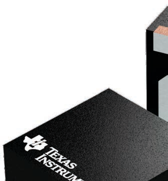
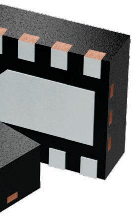

4224783/A www.ti.com

SCALE 5.500
PLASTIC SMALL OUTLINE - NO LEAD 2.1 1.9 A B 0.32 0.18 PIN 1 INDEX AREA
2.1 1.9 0.4 0.2
ALTERNATIVE TERMINAL SHAPE
TYPICAL 0.8 0.7 C
SEATING PLANE
0.05 0.00 0.08 C EXPOSED THERMAL PAD SIDE WALL METAL THICKNESS
DIM A OPTION 2 OPTION 1
0.1 0.2 (DIM A) TYP 0.9 0.1 5 4 6X 0.5 2X 1.5 9 8 1
PIN 1 ID (45 X 0.25)
1.6 0.1 8X 0.4 8X
0.2 0.32 0.18 0.1 0.05 C A B C 4218900/E 08/2022
NOTES:
per ASME Y14.5M.
PLASTIC SMALL OUTLINE - NO LEAD (0.9) 8X (0.5) ( 0.2) VIA
TYP 1 8 8X (0.25)
(0.55) SYMM 9
(1.6)
6X (0.5)
5 4
SYMM (R0.05) TYP (1.9)
LAND PATTERN EXAMPLE
SCALE:20X 0.07 MIN ALL AROUND 0.07 MAX ALL AROUND SOLDER MASK OPENING METAL METAL UNDER
SOLDER MASK NON SOLDER MASK
DEFINED (PREFERRED)
SOLDER MASK OPENING
SOLDER MASK
DEFINED
SOLDER MASK DETAILS 4218900/E 08/2022
NOTES: (continued)
number SLUA271 (www.ti.com/lit/slua271). 5. Vias are optional depending on application, refer to device data sheet. If any vias are implemented, refer to their locations shown
on this view. It is recommended that vias under paste be filled, plugged or tented.
PLASTIC SMALL OUTLINE - NO LEAD 8X (0.5) SYMM METAL
1
8 8X (0.25)
(0.45) SYMM
9 (0.7) 6X (0.5)
5 4
(R0.05) TYP (0.9)
(1.9)
SOLDER PASTE EXAMPLE BASED ON 0.125 mm THICK STENCIL
EXPOSED PAD 9: 87% PRINTED SOLDER COVERAGE BY AREA UNDER PACKAGE
SCALE:25X 4218900/E 08/2022
NOTES: (continued)
design recommendations.
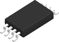
SMALL OUTLINE PACKAGE C 6.6 TYP 6.2 SEATING PLANE
PIN 1 ID AREA A 0.1 C
6X 0.65 8 1
3.1 2.9 NOTE 3 2X 1.95 4
5
B 4.5 4.3
NOTE 4 SEE DETAIL A 8X 0.30 0.19
0.1 C A 1.2 MAX B (0.15) TYP 0.25 GAGE PLANE 0 - 8 0.15 0.05 0.75 0.50
DETAIL A TYPICAL 4221848/A 02/2015 NOTES:
per ASME Y14.5M.
exceed 0.15 mm per side. 4. This dimension does not include interlead flash. Interlead flash shall not exceed 0.25 mm per side.
SMALL OUTLINE PACKAGE 8X (1.5) 8X (0.45) SYMM
1
8 (R 0.05 ) TYP SYMM 6X (0.65)
5 4 (5.8)
LAND PATTERN EXAMPLE
SCALE:10X SOLDER MASK OPENING METAL SOLDER MASK OPENING METAL UNDER SOLDER MASK 0.05 MAX ALL AROUND 0.05 MIN ALL AROUND
SOLDER MASK
DEFINED NON SOLDER MASK
DEFINED
SOLDER MASK DETAILS
NOT TO SCALE 4221848/A 02/2015 NOTES: (continued)
SMALL OUTLINE PACKAGE 8X (1.5) 8X (0.45) SYMM (R 0.05 ) TYP
1
8
SYMM 6X (0.65)
5 4
(5.8)
SOLDER PASTE EXAMPLE BASED ON 0.125 mm THICK STENCIL
SCALE:10X 4221848/A 02/2015 NOTES: (continued)
design recommendations.
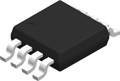
SCALE 4.000
SMALL OUTLINE PACKAGE C 5.05 TYP 4.75 A
0.1 C PIN 1 INDEX AREA SEATING
PLANE 6X 0.65 8 1 2X 3.1 2.9 NOTE 3 1.95 4
5
8X
B 3.1 2.9
NOTE 4 0.38 0.25 0.13 C A B 0.23 0.13 SEE DETAIL A
0.25 GAGE PLANE 1.1 MAX 0 -8 0.15 0.05 0.7 0.4
DETAIL A A 20 TYPICAL 4214862/A 04/2023 PowerPAD is a trademark of Texas Instruments. NOTES:
per ASME Y14.5M.
exceed 0.15 mm per side. 4. This dimension does not include interlead flash. Interlead flash shall not exceed 0.25 mm per side.
SMALL OUTLINE PACKAGE SYMM 8X (1.4)
8X (0.45)
(R0.05) TYP 1 8 SYMM 6X (0.65)
5 4 SEE DETAILS (4.4)
LAND PATTERN EXAMPLE
EXPOSED METAL SHOWN
SCALE: 15X SOLDER MASK
OPENING METAL UNDER SOLDER MASK METAL SOLDER MASK OPENING EXPOSED METAL EXPOSED METAL 0.05 MAX ALL AROUND
NON-SOLDER MASK
DEFINED (PREFERRED)
0.05 MIN ALL AROUND SOLDER MASK
DEFINED SOLDER MASK DETAILS 15.000 4214862/A 04/2023
NOTES: (continued)
on this view. It is recommended that vias under paste be filled, plugged or tented.
SMALL OUTLINE PACKAGE SYMM (R0.05) TYP 8X (1.4)
8X (0.45) 1 8 SYMM 6X (0.65)
5 4 (4.4)
SOLDER PASTE EXAMPLE
SCALE: 15X 4214862/A 04/2023
NOTES: (continued)
design recommendations.
TI PROVIDES TECHNICAL AND RELIABILITY DATA (INCLUDING DATASHEETS), DESIGN RESOURCES (INCLUDING REFERENCE DESIGNS), APPLICATION OR OTHER DESIGN ADVICE, WEB TOOLS, SAFETY INFORMATION, AND OTHER RESOURCES “AS IS” AND WITH ALL FAULTS, AND DISCLAIMS ALL WARRANTIES, EXPRESS AND IMPLIED, INCLUDING WITHOUT LIMITATION ANY IMPLIED WARRANTIES OF MERCHANTABILITY, FITNESS FOR A PARTICULAR PURPOSE OR NON-INFRINGEMENT OF THIRD PARTY INTELLECTUAL PROPERTY RIGHTS. These resources are intended for skilled developers designing with TI products. You are solely responsible for (1) selecting the appropriate TI products for your application, (2) designing, validating and testing your application, and (3) ensuring your application meets applicable standards, and any other safety, security, regulatory or other requirements. These resources are subject to change without notice. TI grants you permission to use these resources only for development of an application that uses the TI products described in the resource. Other reproduction and display of these resources is prohibited. No license is granted to any other TI intellectual property right or to any third party intellectual property right. TI disclaims responsibility for, and you fully indemnify TI and its representatives against any claims, damages, costs, losses, and liabilities arising out of your use of these resources. TI’s products are provided subject to TI’s Terms of Sale, TI’s General Quality Guidelines, or other applicable terms available either on ti.com or provided in conjunction with such TI products. TI’s provision of these resources does not expand or otherwise alter TI’s applicable warranties or warranty disclaimers for TI products. Unless TI explicitly designates a product as custom or customer-specified, TI products are standard, catalog, general purpose devices. TI objects to and rejects any additional or different terms you may propose. IMPORTANT NOTICE Copyright © 2026, Texas Instruments Incorporated
Last updated 10/2025