⬇ Download Markdown · ⬇ Download LaTeX · ⬇ original · view original · CSV: table 1, table 2, table 3
https://doi.org/10.1038/s41586-025-09633-4 Received: 12 January 2025 Accepted: 15 September 2025 Published online: 22 October 2025 Rinsuke Yamada 1,13 ✉ , Max T. Birch 2,13 , Priya R. Baral 1,13 , Shun Okumura 1,2 , Ryota Nakano 1 , Shang Gao 2,12 , Motohiko Ezawa 1 , Takuya Nomoto 3 , Jan Masell 2,4 , Yuki Ishihara 1 , Kamil K. Kolincio 2,5 , Ilya Belopolski 2 , Hajime Sagayama 6 , Hironori Nakao 6 , Kazuki Ohishi 7 , Takashi Ohhara 8 , Ryoji Kiyanagi 8 , Taro Nakajima 2,6,9 , Yoshinori Tokura 1,2,10 , Taka-hisa Arima 2,11 , Yukitoshi Motome 1 , Moritz M. Hirschmann 2 ✉ & Max Hirschberger 1,2 ✉ Check for updates
Antiferromagnetic states with a spin-split electronic structure give rise to spintronic, magnonic and electronic phenomena despite (near-)zero net magnetization 1–7 . The simplest odd-parity spin splitting—p wave—was originally proposed to emerge from a collective instability in interacting electron systems 8–12 . Recent theory has identified a distinct route to realize p-wave spin-split electronic bands without strong correlations 13,14 , termed p-wave magnetism. Here we demonstrate an experimental realization of a metallic p-wave magnet. The odd-parity spin splitting of delocalized conduction electrons arises from their coupling to an antiferromagnetic texture of localized magnetic moments: a coplanar spin helix whose magnetic period is an even multiple of the chemical unit cell, as revealed by X-ray scattering experiments. This texture breaks space-inversion symmetry but approximately preserves time-reversal symmetry up to a half-unit-cell translation—thereby fulfilling the symmetry conditions for p-wave magnetism. Consistent with theoretical predictions, our p-wave magnet shows a characteristic anisotropy in the electronic conductivity 13–15 . Relativistic spin– orbit coupling and a tiny spontaneous net magnetization further break time-reversal symmetry, resulting in a giant anomalous Hall effect (Hall conductivity >600 S cm −1 , Hall angle >3%), for an antiferromagnet. Our model calculations show that the spin-nodal planes found in the electronic structure of p-wave magnets are readily gapped by a small perturbation to induce the anomalous Hall effect. We establish metallic p-wave magnets as an ideal platform to explore the functionality of spin-split electronic states in magnets, superconductors, and in spintronic devices.
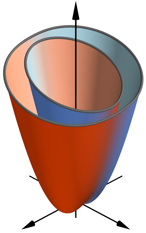
The spin splitting of electronic band states in momentum space is deeply intertwined with the symmetries of magnetic order in direct space 1–5,13 . Uniform ferromagnetic order results in different energies for spin-up (↑) and spin-down (↓) bands, producing a net spin polarization in momentum space that is isotropic across the Fermi surface, as depicted in Fig. 1a. In the language of spherical harmonics, this corresponds to an s-wave state with even parity. In contrast, p-wave spin splitting is characterized in momentum space by an anisotropic spinsplit Fermi surface with collinear ↑ and ↓ states exhibiting odd parity, as shown in Fig. 1b.
In solids, p-wave spin splitting has long been sought as the electronic analogue to the A phase of superfluid helium-3. An initial theoretical route to p-wave spin splitting was proposed in the form of a spin-channel Pomeranchuk instability—a spontaneous Fermi surface distortion driven by electronic correlations that breaks inversion symmetry but preserves the translational symmetry of the system (that is, magnetic modulation vector k mag = 0) 8,9,12 . However, recent theory suggests that p-wave spin splitting also arises when materials form a magnetic superlattice with k mag ≠ 0, where the spin polarization of electronic bands is now considered in the magnetic Brillouin zone 13,14 .
This scenario, termed p-wave magnetism, can be realized without strong electronic correlations and arises when conduction electrons are coupled to an antiferromagnetic texture of localized magnetic moments obeying certain symmetries: time-reversal symmetry T paired with a half-unit cell translation t 1/2 constrains the spin splitting to have odd parity or to vanish, whereas a 180° spin rotation C 2⊥ combined with t 1/2 ensures a unique axis for the spin expectation value of Department of Applied Physics and Quantum-Phase Electronics Center, The University of Tokyo, Tokyo, Japan. 2 RIKEN Center for Emergent Matter Science (CEMS), Wako, Japan. 3 Department of Physics, Tokyo Metropolitan University, Tokyo, Japan. 4 Institute of Theoretical Solid State Physics, Karlsruhe Institute of Technology (KIT), Karlsruhe, Germany. 5 Faculty of Applied Physics and Mathematics, Gdańsk University of Technology, Gdańsk, Poland. 6 Institute of Materials Structure Science, High Energy Accelerator Research Organization, Tsukuba, Japan. 7 Neutron Science and Technology Center, Comprehensive Research Organization for Science and Society (CROSS), Tokai, Japan. 8 J-PARC Center, Japan Atomic Energy Agency, Tokai, Japan. 9 The Institute for Solid State Physics, The University of Tokyo, Kashiwa, Japan. 10 Tokyo College, The University of Tokyo, Tokyo, Japan. 11 Department of Advanced Materials Science, The University of Tokyo, Kashiwa, Japan. 12 Present address: Department of Physics, University of Science and Technology of China, Hefei, China. 13 These authors contributed equally: Rinsuke Yamada, Max T. Birch, Priya R. Baral. ✉ e-mail: [email protected]; [email protected]; [email protected] 1 Nature | Vol 646 | 23 October 2025 | 837
To realize a p-wave magnet based on an evenly commensurate spin helix 13,14 , we focus on the intermetallic compound Gd 3 Ru 4 Al 12 , which is already known to host coplanar spin helices that are incommensurate to the underlying atomic lattice 18–21 , and where the exchange interaction between the localized gadolinium (Gd) moments is mediated by the conduction electrons of ruthenium (Ru). Replacing Ru with rhodium (Rh) and tuning the band filling in Gd 3 (Ru 1−δ Rh δ ) 4 Al 12 , we shift the Fermi level—and thus the period of the magnetic spin helix (Methods and Supplementary Fig. 2). This allows us to approach an N = 6 commensurate spin helix, where both [ T ‖ t 1/2 ] and [ C 2⊥ ‖ t 1/2 ] symmetries are satisfied. Around δ ≈ 0.05, we identify a distinct magnetic ground state, with signatures of p-wave magnetism, as shown in the composition– temperature phase diagram in Fig. 2b.
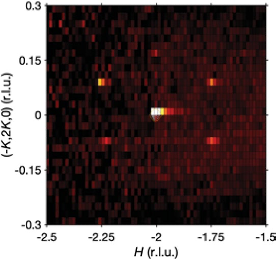
We performed resonant elastic X-ray scattering (REXS) measurements on a series of single crystals with different Rh content δ (Methods). For each sample, we determine the magnetic propagation vector k mag and its orientation relative to the crystal axes. The position of k mag in the Brillouin zone is shown schematically in the inset of Fig. 2b, where blue, red and black symbols indicate k mag for δ = 0, δ = 0.05 and δ = 0.20, respectively. In a narrow composition window around δ ≈ 0.05, we find that the magnetic satellites are indexed as (1/6, 1/6, 0) in Miller notation—indicating that the magnetic period is evenly commensurate with the crystal lattice (N = 6) and consistent with the requirements for p-wave magnetism. The reconstructed unit cell, spanning six crystallographic unit cells, is outlined in red in Fig. 2d. Supporting neutron experiments are shown in Extended Data Fig. 3.
discussion). These X-ray measurements identify the magnetic ground state as a coplanar spin helix, where every magnetic moment rotates within a common m z –m ip plane normal to the spin polarization vector α (shown in Fig. 2i). This magnetic structure preserves the combined spin rotation and translation operation [C 2⊥ ∥t 1/2 ] as well as [ T ‖ t 1/2 ] , and therefore satisfies the symmetry requirements for p-wave magnetism. We stress again that the spin polarization vector α for electronic states in momentum space, introduced in Fig. 1b, is orthogonal to all local magnetic moments in direct space.
One of the predicted consequences of the symmetry-protected p-wave state is in the electronic anisotropy, where the directions parallel and perpendicular to the spin polarization vector α are not equivalent, and we expect to see a resistance that depends on the angle of the applied current relative to the direction of α (refs. 13–15). To probe this, we utilized focused-ion-beam milling to fabricate a freestanding, circular transport device from a single crystal with δ = 0.05. The meandering contacts relieve strain caused by thermal expansion mismatch with the substrate (Fig. 3a and Methods), helping to suppress extrinsic pinning Nature | Vol 646 | 23 October 2025 | 839
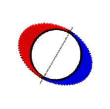
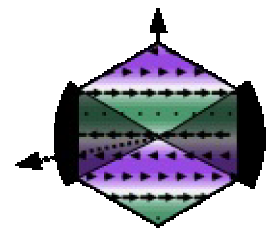
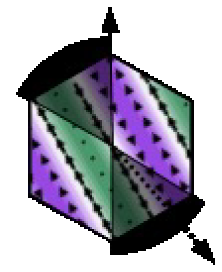
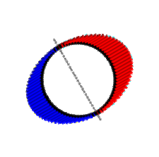
of α. This device enables simultaneous measurement of the resistance along three symmetry-equivalent directions of the hexagonal crystal structure, which become inequivalent upon p-wave magnetic ordering (Fig. 3b). Resistance R xx measured along the crystallographic a axis as a function of temperature is shown in Fig. 3c, revealing magnetic phase transitions consistent with the bulk magnetization (red).
Applying a finite magnetic field perpendicular to the c axis and rotating the sample by the angle ϕ, we observe a characteristic two-fold anisotropic resistivity in Fig. 3d–f. The anisotropy appears only below the magnetic transition, in contrast to the weak, conventional anisotropic resistivity 23 observed in the paramagnetic state (Fig. 3d, white circles). For each magnetic-field direction, one of the three current directions I a , I b or I c shows a higher resistance, whereas the other two have lower resistance. This demonstrates that, for each sextant of the magnetic-field angle ϕ, one of the three magnetic domains characterized by distinct orientations of the spin polarization vector α is selected (Extended Data Fig. 4). Following the conventions of Fig. 1a, the insets in Fig. 3d show the evolution of α in discrete steps during the field rotation, and confirm that current flows more easily along the direction perpendicular to α. In the present compound, the spin-nodal plane is fixed at k x = 0 by symmetry, so the two-fold anisotropic resistivity is directly related to the two-fold symmetry of the p-wave magnet’s spin-split electronic structure (Methods and Supplementary Fig. 13).
approaches the saturation value M sat expected for Gd 3+ moments (Methods), as shown in Fig. 4a. Around zero magnetic field, we observe a small spontaneous magnetization m z of about 2% of M sat with a coercive field of about 0.15 T. Although the p-wave state is slightly distorted when m z becomes finite, the character of p-wave splitting—or ‘p-waveness’ 25 —remains robust in the regime of small m z (Supplementary Figs. 11 and 12). The hysteretic behaviour is discussed in terms of weak exchange anisotropies in Extended Data Fig. 9 and Supplementary Note 8.
As outlined above, we argue that finite spin–orbit coupling in the real material, combined with slight T -breaking of the p-wave bands in momentum space, can generate an intrinsic AHE driven by Berry curvature. Consistent with this expectation, a striking transport response appears when B is parallel to the c axis: with the current in the a–b plane, a sharp, giant anomaly is observed in the Hall conductivity σ xy around B = 0, which is smoothly suppressed as B approaches the critical field B c1 . At higher magnetic field, the Hall effect returns to conventional behaviour, being composed of a magnetization-dependent term with constant S m and a B-linear term from the normal Hall effect with constant S n : σ xy = S n B + S m μ 0 M (ref. 26, Methods and Supplementary Fig. 7). Here μ 0 is the vacuum permeability. The strongly B-dependent contribution Δσ xy in the p-wave state is isolated by subtracting these two terms, and the resulting traces of Δσ xy are shown in Fig. 4c,d. Returning to the minimal low-energy theory presented in equation (1), we model the experimentally observed B-field dependence of the AHE. The result is shown in Fig. 4e, which demonstrates a sharp anomaly in the anomalous Hall conductivity σ xy around zero magnetic field or around zero m z , when ∣ λ ∣ < ∣ p ∣ (Supplementary Note 13). Finally, Fig. 4f compares the zero-field AHE in various bulk antiferromagnets, highlighting the large Δσ xy response in our p-wave candidate, which exceeds 600 S cm −1 — comparable to the intrinsic AHE of ferromagnets. Unlike other antiferromagnets with large AHE and small net magnetization 27–32 , M(B) here
Our p-wave magnet shows a tiny spontaneous magnetization, resulting in a T -breaking distortion of the p-wave electronic structure—a scenario anticipated by models of spin helices of localized magnetic moments coupled to itinerant electrons 24 . Returning to the bulk crystal with δ = 0.05, we set the magnetic field B along the crystallographic c axis and find that the magnetization increases roughly linearly and 840 | Nature | Vol 646 | 23 October 2025 Δ xy (Ω –1 cm –1 )
M sat 500 B || c
Phase II
(IC) 0.04 –0.04
–0.3 b 0 B (T)
5 4 −4 d B c1 1,000
Fig. 4 | Giant AHE induced by a tiny net magnetization m z and spin–orbit coupling. a, Comparison of net magnetization M(B) measured at T = 2 K and T = 20 K. The magnetic field is applied along the c axis. The black triangles correspond to a transition field (B c1 ) from the p-wave magnetic phase (commensurate, C) to the high-temperature phase II (incommensurate, IC; Supplementary Fig. 8). Inset: small spontaneous magnetization m z appears around zero field below B coerc (red triangles) at low temperature. b, Hall A reaching up to conductivity with large zero-field (anomalous) value σ
xy 600 Ω −1 cm −1 , measured on a bulk single crystal (see Extended Data Fig. 5 for the raw data). c, Hall conductivity Δσ xy after subtraction of components proportional to the magnetic field and to the magnetization (Supplementary Fig. 5). Δσ xy is enhanced in the p-wave magnetic phase I. Open circles marking the phase boundaries in c are obtained from magnetization measurements in Extended Data Fig. 7. d, Field dependence of Δσ xy at 2 K and 20 K. Red arrows in d indicate the direction of the field sweep. e, Calculated anomalous Hall conductivity on the k x –k y plane from the low-energy from the low-energy model in equation (1), plotted against m z /p for different values of the chemical potential μ. We consider the breaking of the p-wave state around m z /p ≈ 1.5, where the anomalous Hall conductivity is suppressed to 0 (see Extended Data Fig. 8, Supplementary Fig. 12 and Supplementary Note 13 for details). f, Compared to other bulk antiferromagnets with AHE, our slightly distorted p-wave state
A A induced by m z , large Hall angle tan θ H = σ xy in Gd 3 Ru 4 Al 12 has large σ xy / σ xx and a low saturation magnetic field B sat . Raw data for the bar plot are provided in Extended Data Table 1 (see also Supplementary Table 2).
saturates at modest, accessible fields, enabling practical switching between the p-wave and field-aligned ferromagnetic states.
states in magnets, spintronics, superconductivity and electronic band topology.
Note added in proof: We became aware of the realization of an insulating odd-parity wave magnet after submission of this work 40 . Conclusion The experimentally observed, commensurate spin helix with N = 6 period in direct space satisfies the symmetry requirements for a p-wave magnet up to a tiny, uniform spin splitting m z . This p-wave magnet shows anisotropic electronic properties and a surprisingly large AHE in zero magnetic field. The Hall response is attributed to Berry curvature in momentum space arising when m z opens a gap at the nodal planes of a p-wave magnet. Recent theoretical studies predicted the generation of large linear and nonlinear spin currents in p-wave magnets as well as a large tunnelling magnetoresistance 6,7,15,16,33,34 . In particular, it is believed that the low number of nodal planes in spinsplit p-wave antiferromagnets is advantageous for functionality as a spin injector 16,33 . Expanding on the literature of proximitized spin helices as a route to unconventional superconductivity 35–38 , superconducting proximity effects have also been recently discussed for p-wave magnets 17,39 . Our findings establish metallic p-wave magnets as an ideal platform to explore the interplay of spin-split electronic
Any methods, additional references, Nature Portfolio reporting summaries, source data, extended data, supplementary information, acknowledgements, peer review information; details of author contributions and competing interests; and statements of data and code availability are available at https://doi.org/10.1038/s41586-025-09633-4.
Ahn, K.-H., Hariki, A., Lee, K.-W. & Kuneš, J. Antiferromagnetism in RuO 2 as d-wave Pomeranchuk instability. Phys. Rev. B 99, 184432 (2019). Naka, M. et al. Spin current generation in organic antiferromagnets. Nat. Commun. 10, 4305 (2019). Šmejkal, L., González-Hernández, R., Jungwirth, T. & Sinova, J. Crystal time-reversal symmetry breaking and spontaneous Hall effect in collinear antiferromagnets. Sci. Adv. 6, eaaz8809 (2020). Šmejkal, L., Sinova, J. & Jungwirth, T. Emerging research landscape of altermagnetism. Phys. Rev. X 12, 040501 (2022).
Nature | Vol 646 | 23 October 2025 | 841
antiferromagnetism: a phase with nonrelativistic spin and crystal rotation symmetry. Phys. Rev. X 12, 031042 (2022).
i-wave altermagnets and perfectly nonreciprocal spin current in f-wave magnets. Phys. Rev. B 111, 125420 (2025). 7. Yu, Y. et al. Odd-parity magnetism driven by antiferromagnetic exchange. Phys. Rev. Lett.
135, 046701 (2025).
Phys. Rev. B 75, 115103 (2007). 10. Jung, J., Polini, M. & MacDonald, A. H. Persistent current states in bilayer graphene.
Phys. Rev. B 91, 155423 (2015). 11. Kiselev, E. I., Scheurer, M. S., Wölfle, P. & Schmalian, J. Limits on dynamically generated
spin-orbit coupling: absence of l = 1 Pomeranchuk instabilities in metals. Phys. Rev. B 95, 125122 (2017). 12. Wu, Y.-M., Klein, A. & Chubukov, A. V. Conditions for l = 1 Pomeranchuk instability in a Fermi
liquid. Phys. Rev. B 97, 165101 (2018). 13. Hellenes, A. B. et al. P-wave magnets. Preprint at https://arxiv.org/abs/2309.01607 (2024). 14. Jungwirth, T. et al. From superfluid 3 He to altermagnets. Preprint at https://arxiv.org/abs/
2411.00717 (2024). 15. Ezawa, M. Purely electrical detection of the spin-splitting vector in p-wave magnets based
on linear and nonlinear conductivities. Phys. Rev. B 112, 125412 (2025).
transport properties of unconventional p-wave magnets. Phys. Rev. Lett. 133, 236703 (2024).
electrical control and detection of a domain wall. Phys. Rev. B 110, 165429 (2024). 18. Gladyshevskii, R. E., Strusievicz, O. R., Cenzual, K. & Parthé, E. Structure of Gd 3 Ru 4 Al 12 , a
new member of the EuMg 5.2 structure family with minority-atom clusters. Acta Crystallogr. B 49, 474–478 (1993). 19. Niermann, J. & Jeitschko, W. Ternary rare earth (R) transition metal aluminides R 3 T 4 Al 12
(T = Ru and Os) with Gd 3 Ru 4 Al 12 type structure. Z. Anorg. Allg. Chem. 628, 2549–2556 (2002). 20. Nakamura, S. et al. Spin trimer formation in the metallic compound Gd 3 Ru 4 Al 12 with a
distorted kagome lattice structure. Phys. Rev. B 98, 054410 (2018). 21. Matsumura, T., Ozono, Y., Nakamura, S., Kabeya, N. & Ochiai, A. Helical ordering of spin
trimers in a distorted kagomé lattice of Gd 3 Ru 4 Al 12 studied by resonant X-ray diffraction. J. Phys. Soc. Jpn 88, 023704 (2019). 22. Lovesey, S. W. & Collins, S. P. X-ray Scattering and Absorption by Magnetic Materials Oxford
Series on Synchrotron Radiation No. 1 (Clarendon Press, Oxford Univ. Press, 1996).
IEEE Trans. Magn. 11, 1018–1038 (1975). 24. Okumura, S., Kato, Y. & Motome, Y. Lock-in of a chiral soliton lattice by itinerant electrons.
J. Phys. Soc. Jpn 87, 033708 (2018).
842 | Nature | Vol 646 | 23 October 2025 25.
Hodt, E. W., Bentmann, H. & Linder, J. Fate of p-wave spin polarization in helimagnets with Rashba spin-orbit coupling. Phys. Rev. B 111, 205416 (2025) Nagaosa, N., Sinova, J., Onoda, S., MacDonald, A. H. & Ong, N. P. Anomalous Hall effect. Rev. Mod. Phys. 82, 1539 (2010). Nakatsuji, S., Kiyohara, N. & Higo, T. Large anomalous Hall effect in a non-collinear antiferromagnet at room temperature. Nature 527, 212–215 (2015). Nayak, A. K. et al. Large anomalous Hall effect driven by a nonvanishing Berry curvature in the noncolinear antiferromagnet Mn 3 Ge. Sci. Adv. 2, e1501870 (2016). Ghimire, N. J. et al. Large anomalous Hall effect in the chiral-lattice antiferromagnet CoNb 3 S 6 . Nat. Commun. 9, 3280 (2018). Takagi, H. et al. Spontaneous topological Hall effect induced by non-coplanar antiferromagnetic order in intercalated van der Waals materials. Nat. Phys. 19, 961–968 (2023). Park, P. et al. Tetrahedral triple-Q magnetic ordering and large spontaneous Hall conductivity in the metallic triangular antiferromagnet Co 1/3 TaS 2 . Nat. Commun. 14, 8346 (2023). Šmejkal, L., MacDonald, A. H., Sinova, J., Nakatsuji, S. & Jungwirth, T. Anomalous Hall antiferromagnets. Nat. Rev. Mater. 7, 482–496 (2022). Hedayati, A. A. & Salehi, M. Transverse spin current at normal-metal /p-wave magnet junctions. Phys. Rev. B 111, 035404 (2025). Álvarez Pari, N. A., Jaeschke-Ubiergo, R., Chakraborty, A., Šmejkal, L. & Sinova, J. Nonrelativistic linear Edelstein effect in helical EuIn 2 As 2 . Phys. Rev. B 112, 024404 (2025). Choy, T. P., Edge, J. M., Akhmerov, A. R. & Beenakker, C. W. J. Majorana fermions emerging from magnetic nanoparticles on a superconductor without spin–orbit coupling. Phys. Rev. B 84, 195442 (2011). Martin, I. & Morpurgo, A. F. Majorana fermions in superconducting helical magnets. Phys. Rev. B 85, 144505 (2012). Nadj-Perge, S., Drozdov, I. K., Bernevig, B. A. & Yazdani, A. Proposal for realizing Majorana fermions in chains of magnetic atoms on a superconductor. Phys. Rev. B 88, 020407 (2013). Klinovaja, J., Stano, P., Yazdani, A. & Loss, D. Topological superconductivity and Majorana fermions in RKKY systems. Phys. Rev. Lett. 111, 186805 (2013). Maeda, K., Lu, B., Yada, K. & Tanaka, Y. Theory of tunneling spectroscopy in unconventional p-wave magnet-superconductor hybrid structures. J. Phys. Soc. Jpn 93, 114703 (2024). Song, Q. et al. Electrical switching of a p-wave magnet. Nature 642, 64–70 (2025).
Publisher’s note Springer Nature remains neutral with regard to jurisdictional claims in published maps and institutional affiliations.
Springer Nature or its licensor (e.g. a society or other partner) holds exclusive rights to this article under a publishing agreement with the author(s) or other rightsholder(s); author selfarchiving of the accepted manuscript version of this article is solely governed by the terms of such publishing agreement and applicable law.
© The Author(s), under exclusive licence to Springer Nature Limited 2025, corrected publication 2025
Crystal growth and characterization Single crystals of Gd 3 (Ru 1−δ Rh δ ) 4 Al 12 were synthesized under argon gas flow in a high-vacuum floating zone furnace. The sample quality was confirmed by powder X-ray diffraction (Supplementary Fig. 1 and Supplementary Table 1), energy-dispersive X-ray spectroscopy and by examination under an optical polarization microscope. We used Laue X-ray diffraction and a diamond saw to precisely orient and align the sample surfaces.
Magnetization and electrical transport measurements on bulk samples Magnetization was measured in a commercial Quantum Design MPMS3 (DC-mode) and Quantum Design PPMS-14T (VSM, vibrating sample magnetometer). The magnetic field was applied along the crystallographic c axis of the crystal. Electrical transport measurements were performed on polished single-crystal plates with electrical contacts made of 30-μm gold wires, using silver paste (Dupont). We set the sample surface perpendicular to the c axis (B∥c) and applied the electric current along the a axis to measure the data in Fig. 3. We performed a demagnetization correction by assuming that the sample shape is an ellipse to compare field-dependent physical properties of samples with different shapes 41 .
Focused-ion-beam device fabrication and measurements Using a Thermo Fischer Helios 5UX focused-ion-beam system, a lamella was carved and extracted from the bulk crystal, thinned down and shaped into a circle. Using an in situ micro-manipulator, this circle was placed on to an aluminium oxide (Al 2 O 3 ) substrate patterned with Au contacts, and attached with ion-beam-induced Pt deposition. The meander-shaped bonds and final sample geometry were created with a final ion-milling step. The entire device was coated in a capping layer of 5 nm of Al 2 O 3 using atomic layer deposition. The anisotropic resistance of the finished device was measured in a Quantum Design PPMS-14T as described in the previous paragraph, using the as-provided rotator probe option. We confirmed that the transport properties of the device well reproduce those of bulk single crystals, as shown in Extended Data Fig. 6.
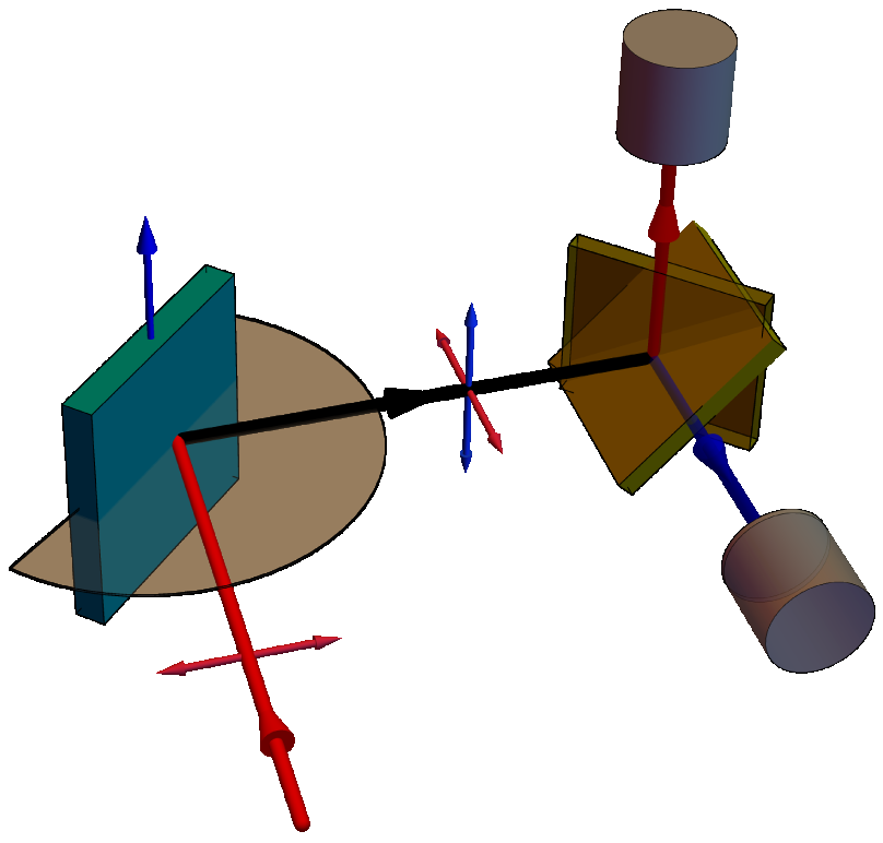
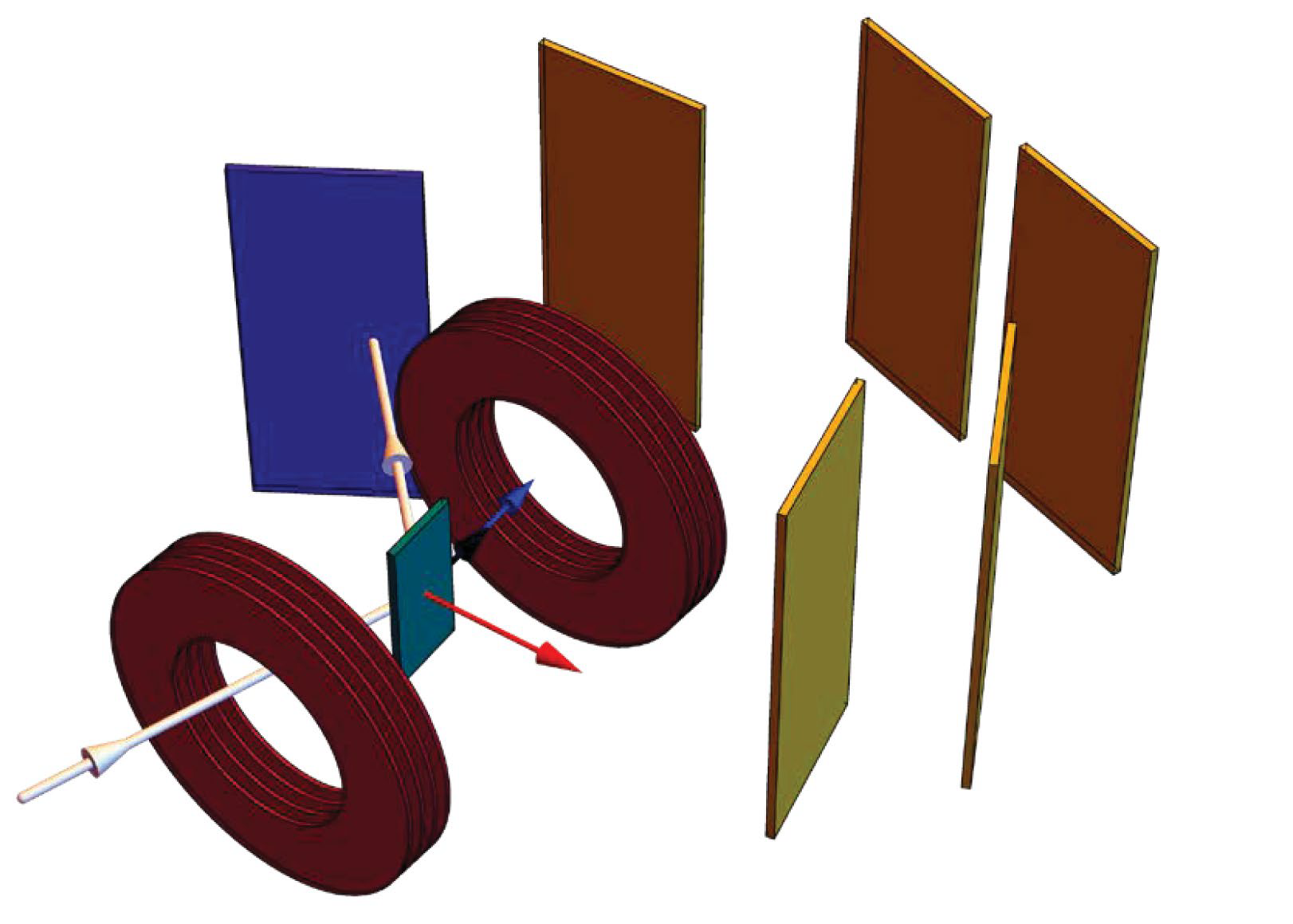
Resonant elastic X-ray scattering Magnetic REXS experiments were conducted at BL-3A (KEK, Photon Factory, Japan) using the Gd-L 2 absorption edge. The scattering plane is (H, K, 0), so that the incoming and outgoing beam wavevectors k i and k f are perpendicular to the crystallographic c axis. We used the (006) reflection of a pyrolytic graphite plate (2θ ≈ 88° at the Gd-L 2 edge) to perform polarization analysis of the scattered X-ray beam (see Fig. 2c and Supplementary Note 7 for more details). We defined the orientation of the detector with respect to the scattering plane by an angle γ such that γ = 0° detects the π–σ′ component of the scattered X-ray beam, whereas the π–π′ component is detected in the out-of-plane orientation of the detector at γ = 90°.
p-wave spin splitting In this work, we consider collinear spin splitting in the magnetic Brillouin zone of momentum space, that is, spin-split electronic states with a single non-zero component of the spin expectation value ⟨ S x ⟩ ≠ 0 , ⟨ S y ⟩ = ⟨ S z ⟩ = 0 . ⟨ S x ⟩ > 0 and ⟨ S x ⟩ < 0 are labelled as ↑ and ↓, respectively, although ∣ ⟨ S x ⟩ ∣ < ℏ /2 is allowed, where ℏ is the Planck constant divided by 2π. In the low-energy limit, the electronic band structure has an energy gap of approximately cos( lθ q ) between the ↑ and ↓ bands in momentum space, with l = 0, 1 and 2 for s-, p- and d-wave spin splitting, respectively. The azimuthal angle θ q is the angle of q relative to the x axis 9 ; q = k − k TRIM is measured from the position of the TRIM (time reversal invariant momenta) around which the low-energy model is expanded (Supplementary Note 15).
Collinear spin expectation value in momentum space We use the symmetries of the present material with a six-fold expanded magnetic unit cell (N = 6) to discuss the spin polarization of conduction electron states in momentum space. Here spin-space group symmetries are denoted as [ S ‖ R ], where S acts on spin space and R applies to real space, whereas operators without brackets are used to refer to specific (matrix) representations of symmetry operations. In the present material, the symmetry [C 2⊥ ∥t 1/2 ] is equivalent to [C 2x ∥t 1/2 ] and all bands and eigenstates can be labelled using its symmetry eigenvalues λ s . We introduce the composite operator U s t 1/6 with the intention of defining the 2 π S λ s : a six-fold spin rotation around the x axis, U s = exp(i 6 ℏ
x ) , combined with a translation t 1/6 = a o /6 + b o /2. Here, S x is the spin-1/2 operator component. We use the lattice vectors a o and b o of the magnetic unit cell (orthorhombic), with lattice constants a o and b o —as in Fig. 2d.
Let a Hamiltonian of conduction electrons be exchange-coupled to the magnetic state discussed in the main text. Without spin–orbit 2 S ∼ coupling (SOC), this Hamiltonian commutes with ( U
s t 1/6 )
3 = i
ℏ x t 1/2 ≡ S x . ∼ The energy eigenstates ∣E , λ s ⟩ are also eigenstates of S x with eigenvalue ∼ ∼ ∼
Low-energy model from symmetries Starting from the point-group symmetries of p-wave magnets, we construct a low-energy model describing an electronic band in three dimensions, coupled to the magnetic texture. The model represents the low-energy limit of the electronic structure of a p-wave magnet in the magnetic Brillouin zone. For such an expansion around k = 0, the symmetries [C 2x ∥t 1/2 ] and [ T ‖ t 1/2 ] are represented by C 2x = iσ x and T = i σ y K , respectively, with the complex conjugation K. Without SOC, the Hamiltonian is required to commute with C 2x , and, further, is required to be consistent with time-reversal symmetry T −1 H ( k ) T = H (− k ) . To linear order, all allowed terms are equivalent to pk x σ x . As for SOC, we consider leading-order terms that are allowed owing to broken inversion symmetry and breaking of all mirror planes in the p-wave state. The spin rotation C 2x can now be broken and any term of the form k i σ j with i, j ∈ {x, y, z} is consistent with T . However, SOC does not break a combined rotation [C 2x ∥C 2x t 1/2 ] in spin and direct spaces, which is characteristic for the magnetic state depicted in Fig. 2i. Among the remaining symmetry-allowed in-plane terms, k x σ y , k y σ y , k x σ z and k y σ z , the k x -dependent terms are expected to be negligible compared with the p-wave splitting. As k y σ z and k y σ y are equivalent in their effect on spin splitting, we include only k y σ y , which is needed for a non-zero AHE. Finally, the kinetic energy of a parabolic band is k 2 σ 0 and the Zeeman-type energy in an exchange field along the z axis is ∝ σ z . These considerations lead to equation (1), which can be rewritten in terms of the vector d as
i (2)
electrons coupled to a commensurate spin helix composed of 4f local magnetic moments. This calculation is shown in Supplementary Fig. 14 and Supplementary Notes 9 and 10.
Spin-nodal plane in momentum space In the following, we make some more general remarks on the electronic structure of the p-wave magnet. We can argue for the existence of dege nerate nodal planes in momentum space by invoking T symmetry on
∼ the eigenstates of S x = ( U s t 1/6 ) 3 with eigenvalues ±λ s . The T operation comprises complex conjugation of wavefunctions and a spin flip, so ∼ ∼ we have T S x = S x T . This yields E(k) = E(−k), as two eigenstates of the Hamiltonian are related by T ∣ E , k , λ s ⟩ ∝ ∣ E , − k , − λ s ⟩ with T λ s = − λ s T . The λ s is a good quantum number for all crystal momenta k; hence, along any line connecting the momenta k and −k, there must be an odd number of exchanges between eigenstates labelled by +λ s and −λ s . This implies an odd number of nodal planes on which the energy bands of the Hamiltonian are twofold degenerate in absence of SOC.
Pinning of nodal plane to high-symmetry directions We discuss symmetry constraints that force the nodal planes to be flat and spanned by high-symmetry directions in k space. Again invoking the [C 2x ∥C 2x t 1/2 ] symmetry and combining with [ T ‖ t 1/2 ] , we define their product G = [ C 2 x T C 2 x ] . This G commutes with the Hamiltonian and with [C 2x ∥t 1/2 ] up to a full lattice translation. In addition, G acts on crystal momenta like a mirror operation, (k x , k y , k z ) → (−k x , k y , k z ) and exchanges the sign of λ s by complex conjugation. Thus, G enforces a nodal plane at k x = 0, where the eigenvalues ±λ s label states of degenerate energy. Extended Data Fig. 4 and Supplementary Fig. 3 discuss the two-fold symmetric anisotropic magnetoresistance attributed to electronic anisotropy and the pinned spin-nodal plane in our p-wave magnet.
Electronic-structure calculations We performed spin density functional theory (DFT) calculations for Gd 3 Ru 4 Al 12 (Supplementary Fig. 10). The calculations were carried out using the projector augmented-wave method as implemented in the Vienna Ab initio Simulation Package 42 , together with the generalized gradient approximation for the exchange-correlation functional proposed by Perdew, Burke and Ernzerhof 43 . The crystal structure data were adopted from ref. 18. In the electronic-structure calculations, we used a plane-wave energy cut-off of 400 eV and a 9 × 9 × 9 Monkhorst–Pack k-point grid. All calculations were performed assuming a ferromagnetically ordered state. To account for the strong correlation effects in the Gd 4f orbitals, we used the DFT + U approach, setting the on-site Coulomb interaction U to 6.7 eV and the Hund’s coupling J to 0.7 eV (refs. 44,45).
All experimental data to reproduce the figures are available on Zenodo at https://doi.org/10.5281/zenodo.17035626 (ref. 46).
The source code used to perform the calculations described in this paper is available from the corresponding authors upon request.
83, 3432–3434 (1998). 42. Kresse, G. & Furthmüller, J. Efficient iterative schemes for ab initio total-energy calculations
using a plane-wave basis set. Phys. Rev. B 54, 11169 (1996). 43. Perdew, J. P., Burke, K. & Ernzerhof, M. Generalized gradient approximation made simple.
Phys. Rev. Lett. 77, 3865–3868 (1996).
magneto-optical properties for 4f systems: LSDA + Hubbard U results. J. Phys. Chem. Solids 56, 1521–1524 (1995). 45. Shick, A. B., Liechtenstein, A. I. & Pickett, W. E. Implementation of the LDA+U method using
the full-potential linearized augmented plane-wave basis. Phys. Rev. B 60, 10763–10769 (1999).
https://doi.org/10.5281/zenodo.17035626 (2025).
antiferromagnet. Nat. Phys. 13, 1085–1090 (2017).
non-collinear magnet Mn 3 Ga. Sci. Rep. 7, 515 (2017). 50. Hayashi, H. et al. Large anomalous Hall effect observed in the cubic-lattice antiferromagnet
Mn 3 Sb with kagome lattice. Phys. Rev. B 108, 075140 (2023). 51. Zuniga-Cespedes, B. E. et al. Observation of an anomalous Hall effect in single-crystal
Mn 3 Pt. New J. Phys. 25, 023029 (2023). 52. Sürgers, C. et al. Anomalous Nernst effect in the noncollinear antiferromagnet Mn 5 Si 3 .
Commun. Mater. 5, 176 (2024).
orthorhombic antiferromagnetic material NbMnP. npj Quantum Mater. 8, 56 (2023).
antiferromagnetic material TaMnP. Phys. Rev. B 110, 214417 (2024). 55. Kotegawa, H. et al. Large anomalous Hall conductivity derived from an f-electron collinear
antiferromagnetic structure. Phys. Rev. Lett. 133, 106301 (2024).
Acknowledgements We acknowledge A. Kikkawa for help with crystal growth. We acknowledge support from the Japan Society for the Promotion of Science (JSPS) under grant numbers JP22H04463, JP23H05431, JP22F22742, JP22K20348, JP23K13057, JP23H00171, JP24H01607, JP24H01604, JP25K17336, JP22K13998, and JP23K25816, and from the Murata Science Foundation, Yamada Science Foundation, Hattori Hokokai Foundation, Mazda Foundation, Casio Science Promotion Foundation, Inamori Foundation, Kenjiro Takayanagi Foundation, Foundation for Promotion of Material Science and Technology of Japan, Yashima Environment Technology Foundation, Yazaki Memorial Foundation for Science and Technology, and ENEOS Tonengeneral Research/Academic Foundation. This work was partially supported by the Japan Science and Technology Agency via JST CREST grant numbers JPMJCR1874, JPMJCR20T1 and JPMJCR20T2 (Japan), JST FOREST (JPMJFR2238), and JST PRESTO (JPMJPR259A, JPMJPR2595). It was also supported by Japan Science and Technology Agency (JST) as part of Adopting Sustainable Partnerships for Innovative Research Ecosystem (ASPIRE), grant number JPMJAP2426. M.H. is supported by the Deutsche Forschungsgemeinschaft (DFG, German Research Foundation) via Transregio TRR 360 – 492547816. P.R.B. acknowledges Swiss National Science Foundation (SNSF) Postdoc.Mobility grant P500PT_217697 for financial assistance. M.M.H. is funded by the Deutsche Forschungsgemeinschaft (DFG, German Research Foundation) project number 518238332. J.M. acknowledges funding from the DFG under the project number 547968854. Resonant X-ray scattering at Photon Factory (KEK) was carried out under proposal numbers 2022G551 and 2023G611. The neutron experiments at the Materials and Life Science Experimental Facility of J-PARC were performed under a user programme (proposal number 2020B0347, TAIKAN, and number 2020A0282, SENJU).
Author contributions M.H., Y.M., T.-h.A. and Y.T. conceived of the project. R.Y. and M.H. grew and characterized the single crystals. R.Y., R.N. and M.H. performed the magnetization and transport measurements on bulk samples. M.T.B. prepared the focused-ion-beam devices and performed all the device measurements. P.R.B., R.N., S.G., H.S., H.N. and M.H. performed the resonant X-ray scattering experiments and analysed the data with guidance from T.-h.A. T. Nakajima, K.O., K.K.K., T.O., R.K. and M.H. performed the neutron scattering experiments, and the data were analysed by P.R.B. and Y.I. S.O., M.M.H., M.E., J.M. and Y.M. performed the symmetry analysis and model calculations. T. Nomoto performed the ab initio calculations. R.Y., M.T.B., P.R.B. and M.H. wrote the paper with help from I.B. All authors discussed the results and commented on the paper.
Competing interests The authors declare no competing interests.
Additional information Supplementary information The online version contains supplementary material available at https://doi.org/10.1038/s41586-025-09633-4. Correspondence and requests for materials should be addressed to Rinsuke Yamada, Moritz M. Hirschmann or Max Hirschberger. Peer review information Nature thanks the anonymous reviewers for their contribution to the peer review of this work. Reprints and permissions information is available at http://www.nature.com/reprints.
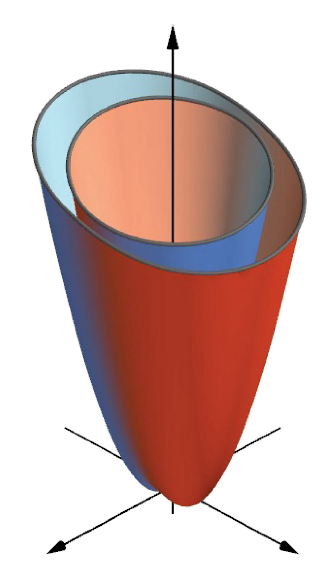
Extended Data Fig. 1 | Fermi surfaces of a p-wave band. a, Band dispersion with p-wave splitting, spin-orbit coupling (SOC), and time-reversal breaking m z = 0.01. Here, we set p = 1.2 and λ = 0.4, where p-wave exchange splitting is larger than the size of SOC and the net magnetization is small but non-zero. b,c, Fermi surfaces of a p-wave split band with (m z = 0, λ = 0) and without (m z = 0.01, λ = 0.4) time-reversal symmetry, respectively. The two bands are degenerate on the k x = 0 plane for m z = 0. However, the degeneracy is lifted due to band hybridization when m z is finite in Eq. (1). The equal energy surface is calculated at E = 10 in panels (b, c). Contrary to the low-energy model for a p-wave Pomeranchuk instability, ∣ ⟨ S x ⟩ ∣ < ℏ /2 for the p-wave magnet of conduction electrons coupled to a spin helix (Methods, Supplementary Fig. 15 and Note 15).
Extended Data Fig. 2 | Resonant elastic X-ray scattering of magnetic (1) satellites in Phase-I. a, The magnetic reflection intensity at Q
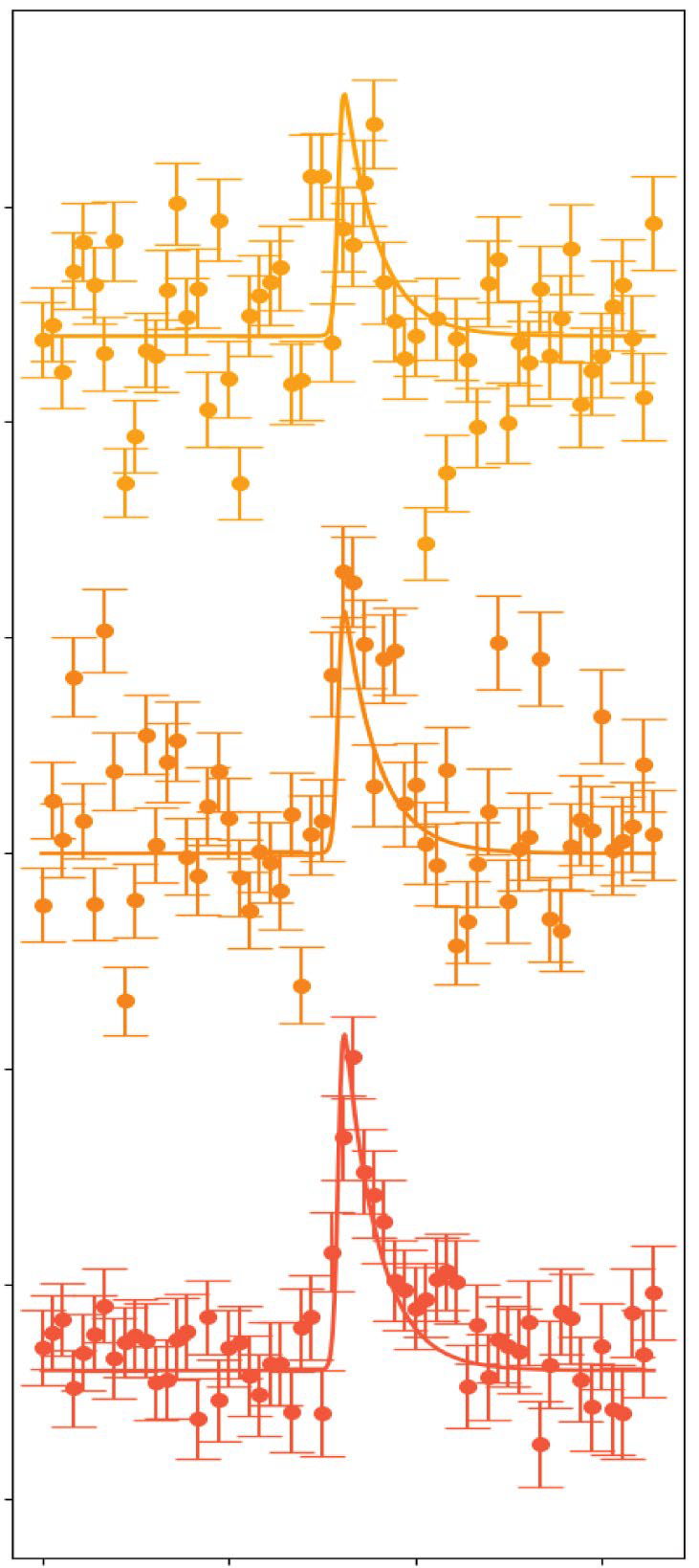
M (≡ G 440 − k mag ) and total fluorescence signal obtained at T = 4 K strongly depend on the energy E of the incoming synchrotron X-ray beam. The maximum intensity due to magnetic scattering appears at E = 7.935 keV, in resonance with the Gd-L 2 absorption edge. Inset: schematic of momentum space and magnetic satellites around the (440) fundamental (structural) reflection. We indicate the center of momentum space, Γ, and lattice vectors of momentum space. b, Measurement geometry for detecting the Q M reflection: k i and k f are the wavevectors of the incoming and outgoing X-ray beams, respectively. The angles ω, 2θ defined here are referred to in Eq. (S5) and following in Supplementary Note 7. c, Polarisation analysis of magnetic satellites close to (440), (250), and (700) fundamental reflections using Eq. (S6) in Supplementary Note 7 reveals good agreement with a distorted spin helix model. Dashed green (yellow) lines represent expected behaviour for a harmonic cycloid (harmonic helix). The data are consistent with a distorted helix, elliptically squeezed into the hexagonal basal plane. Even when the commensurate helix shows a distorted spin rotation plane, the symmetries [C 2x ∥t 1/2 ] and [ T ∥t 1/2 ] are preserved.

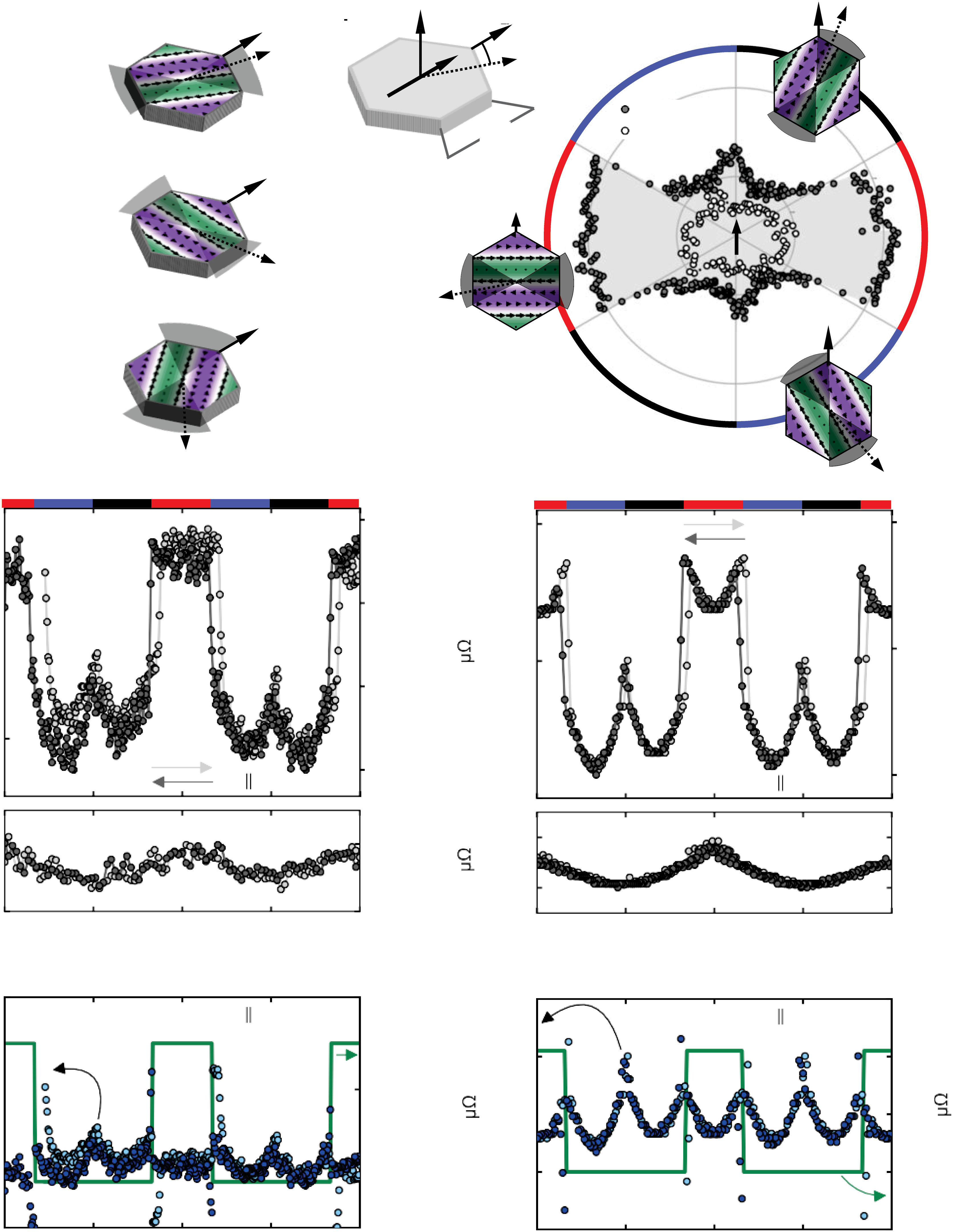
Extended Data Fig. 4 | Step-like anisotropic magnetoresistance due to switching of p-wave domains, corresponding to switching the spin polarisation vector α. a-c, Three types of α-domain configurations that can be controlled by rotating the magnetic field in the ab-plane. The relative angle between the a-axis and B is ϕ. The gray shaded wedges indicate the range of angles where a given domain is stable: ϕ = 0° ~ 60° (180° ~ 240°), 60° ~ 120° (240° ~ 300°), and 120° ~ 180° (300° ~ 360°), respectively, for Configuration 1, 2, and 3. d, Polar plot of AMR with illustrations of α-domain configurations. Step-like AMR observed in the p-wave phase originating from the switching of a α-domains (see Supplementary Fig. 9). For current I
a ∥a, a higher resistance R xx appears in Configuration 2 (red region), where I is nearly parallel to α. We also show the measurement configuration of anisotropic magnetoresistance (AMR). The current I a is applied along the a-axis, while the magnetic field B is rotated within the ab-plane. e,f, AMR of a fabricated device with strain relief at T = 2 K and 30 K. The second y-axis on the right-hand side shows the relative magnitude of the AMR. g,h, AMR of a bulk sample at T = 2 K and 30 K. Bulk and device curves are in good qualitative agreement, although the AMR’s relative magnitude is three times larger in the suspended device. We note that the AMR measurement on devices allows us to measure the resistivity along several current directions simultaneously (see Fig. 3, Main Text). i,j, Separation of AMR into (i) step-type anomaly related to resistivity anisotropy in the p-wave magnet (green line, right axis) and (ii) six-fold patterns with the periodicity of the underlying crystal lattice (blue symbols, left axis). As the relative magnitude of the p-wave AMR is larger in the device, the six-fold patterns are harder to distinguish. Arrows in e,g indicate the sweep direction of the magnetic-field angle ϕ.
Extended Data Fig. 5 | Electrical resistivity and Hall resistivity data for a bulk single crystal of Gd 3 (Ru 0.95 Rh 0.05 ) 4 Al 12 . a-c, Longitudinal resistivity ρ x x , Hall resistivity ρ yx , and Hall conductivity σ xy at various temperatures. In support of Fig. 4 of the Main Text, here we show raw data of each quantity. Direction of magnetic field ramping is indicated by black arrows, with solid lines for ∂B/∂t < 0 and dashed lines for increasing magnetic field. The magnetic field is applied along the c-axis of the crystal. The offset between curves is set to be 2 μΩcm, 2 μΩcm, and 500 Ω −1 cm −1 in panels a, b, and c, respectively.
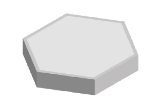
Extended Data Fig. 6 | Comparing transport properties of bulk single crystal and suspended device at T = 2 K. The electric current and magnetic field are applied along the a-axis and c-axis, respectively. a Longitudinal resistivity ρ x x for a device fabricated by the focused ion beam technique. b, c Magnetic field dependence of Hall resistivity ρ yx and longitudinal conductivity σ x x . d Hall conductivity σ xy calculated for the device (red/blue) and for the bulk single crystal (gray line). The data are in good qualitative agreement. Inset: schematic measurement geometry. The hysteresis in ρ xx and σ xx is attributed to the texture of p-wave domains, as discussed further in Supplementary Fig. 4. To calculate the conductivities and resistivities of the device, we approximate the width and length of the central circular patch as a rectangular bar, implying significant systematic errors due to the geometry of the device. Note: The Hall conductivity data presented in the Main Text was obtained from bulk single crystals to suppress systematic measurement errors for the absolute value of σ xy .
Extended Data Fig. 7 | Bulk magnetization data with B∥c. a, Curie-Weiss fit of magnetic susceptibility χ = M/H, measured with 0.1 T external magnetic field applied along the c-axis. b, M(H) curves obtained at constant temperatures T as indicated in the panel. c, Magnetization isotherm and its corresponding field derivative at T = 2 K. The dashed vertical line, labelled as B c1 , represents the hysteretic boundary between Phase-I and Phase-II. Around this region, ramping up and ramping down direction of external magnetic field is indicated by solid and dashed arrows, respectively. d, Derivative of magnetization with respect to applied field at various T, showing peak-like features at B coerc (red arrow) and B c1 (black arrows) defined in Fig. 4a. Consecutive curves are shifted by 0.2 μ B f.u. −1 T −1 for better visibility. Similar to Panel-c, solid and dashed lines denote the direction of magnetic field ramping. e, Temperature dependent derivative dM/dT of magnetization data measured at constant magnetic field, showing two clear transitions, T N1 and T N2 as defined in Fig. 3. Each consecutive curve is shifted by 0.002 emu mol −1 K −1 for better visibility. Inset: Zoom-in of data at low magnetic field.
Extended Data Fig. 8 | Anomalous Hall conductivity of a distorted p-wave magnet. Anomalous Hall conductivity as a function of the uniform net magnetization S k z =0 . Here, S 0 is the total length of the magnetic moment (saturation moment). In the low-energy model, only m z is varied while p = 0.1, k B T = 0.04 – as well as spin-orbit coupling strength λ and chemical potential μ, written in each panel – are fixed. We calculate S k z =0 from m z /p and the parameters J, t of a tight-binding Hamiltonian, as described in Supplementary Note 12. A sharp anomaly emerges for small S k z =0 when λ is weak, λ/p < 1. In the gray region, the spin helix collapses as discussed in Supplementary Note 13.
Extended Data Fig. 9 | Solitonic spin states with a net magnetization from biquadratic magnetic interactions, following Supplementary Note 8. To explain the observed distorted spin helix state with a weak net magnetization, we develop a simple 1D two-parameter model in Eq. (S8) in Supplementary Note 8. In this model, we introduce the exchange anisotropy Δ > 0 and Δ′ > 0 to favour a spin helix with net magnetization along the z-axis; we also use the RKKY interaction J = 1, and the four spin interaction K. We optimize the energy to obtain the ground state of the model by simulated annealing. This figure shows the calculation results obtained for Δ = 0.1. Magnetic states with higher harmonics and spontaneous magnetization appear when the four-spin interaction is sufficiently large, K > 0.25.
est A Extended Data Table 1 | Comparison of anomalous Hall conductivity σ xy in zero-field and saturation magnetic field B sat among bulk single crystalline antiferromagnets with small net magnetization
Material Spin texture q-vector est B sat A σ xy
| Material | Spin texture | q-vector | Bsat est | σxy A | σxy A / σxx | Tmax | Ref. |
|---|---|---|---|---|---|---|---|
| (r.l.u.) | (T) | (Ω−1 cm−1 ) | (%) | (K) | |||
| Gd3 (Ru0.95 Rh0.05 )4 Al12 | non-collinear | (6 1 ,6 1 ,0 ) | 5.5 | 600 | 4.2 − 4.7 | 2 | This work |
| Mn3 Sn | non-collinear | (0, 0, 0) | 660 | 20 − 140 | 0.4 − 2.4 | 2 | 27,47 |
| Mn3 Ge | non-collinear | (0, 0, 0) | 1500 | 15 − 350 | 0.4 − 3.6 | 2 | 28,48 |
| Mn3 Ga | non-collinear | (0, 0, 0) | 180 | 18 | 0.5 | 300 | 49 |
| Mn3 Sb | non-collinear | (0, 0, 0) | 650 | 310 | 1.1 − 1.5 | 150 | 50 |
| Mn3 Pt | non-collinear | (0, 0, 0) | 2445 | 100 | 0.8 | 120 | 51 |
| CoNb3 S6 | non-coplanar | (2 1 , 0, 0 ) | 250 | 27 | 0.7 | 23 | 29 |
2 170 75 − 135 0.9 − 1.6 6 30,31 Mn 5 Si 3 non-coplanar 1
2 180 160 2.3 25 52 NbMnP non-collinear ( , 0, 0 ) ( , 0, 0 ) ( , 0, 0 ) (0, 0, 0) 1100 230 1.9 − 3.2 2 53 TaMnP non-collinear (0, 0, 0) 1200 370 1.4 − 2.7 2 54 Ce 2 CuGe 6 collinear (0, 0, 0) 90 550 0.2 1.3 55 Gd 3 (Ru 0.95 Rh 0.05 ) 4 Al 12 non-collinear Mn 3 Sn non-collinear Mn 3 Ge
−1 −1 Gd 3 (Ru 0.95 Rh 0.05 ) 4 Al 12 shows a commensurate non-collinear spin texture, a giant anomalous Hall conductivity, and a large Hall angle. It also has a low magnetic field for transition into the A takes a maximum value. Error bar of A ferromagnetic state, simplifying the data analysis. T max is a temperature where σ xy σ xy / σ xx in our material is estimated from the variation of the values A and A A between a bulk sample and a device. As for Mn 3 Sn and Mn 3 Ge, error bars for σ xy σ xy / σ xx indicate variation of the values for different field directions. Since σ xy / σ xx of Mn 3 Sb, NbMnP, and A , we added error bars for these compounds. As for CoTa S , error bars are added because there is a variation in reported TaMnP takes a maximum at temperatures different from T max of σ xy 3 6 A . In Fig. 4f, we use A and A A values of σ xy σ xy σ xy / σ xx at T max , and also add error bars for σ xy / σ xx based on this table. References 47–55.