⬇ Download Markdown · ⬇ Download LaTeX · ⬇ original · view original · CSV: table 1
Pradeep Kumar Chawda Texas Instruments Inc., 3833 Kifer Rd, Santa Clara, CA
E-mail: [email protected] equations do not directly include the geometries of the PCB coil in to consideration such as layer stack information. A detailed analysis of various geometrical parameters to performance parameters is required in order to design an optimal multi-layer multi shape PCB coil. In general multiple iterations are required to arrive at optimal solution. This is mainly because a well-defined tool, flow or methodology for designing multi-layer multi-shape PCB coils does not exist for system level applications.
PCB coil design methodologies reported in literature make use of simulated data to study the variation of inductance of the coil with physical parameters of the coil [1]. These methodologies require the simulations to be run every time the setup is changed, and several iterations for a given application. This is time consuming and error prone. Accurate expressions for planer spiral coils are discussed in [2-7]. These need to be extended to include stack layer details for multi-layer coils.
In this paper, an automated flow to efficiently design optimal multi-layer multi-shape PCB coils for system level applications is presented. The flow dynamically derives the relation between output parameters e.g. inductance and the input parameters e.g. coil geometry for given system level specification using well established mathematical model of PCB coil. Representing these relations graphically to PCB designer reduces number of iterations in arriving at correct input parameters for required output parameters and therefore enables much faster coil design as compared to conventional methods. Multiple solutions for the same design specification can now easily be found by varying different input parameters for required output parameters using trade-off plots.
The flow also takes in to account constraints like via connections in the center of the coil well ahead in the calculations for minimum inner diameter in order avoid any iteration later. Step-by-step instructions on how to find optimal solution for a given optimization criteria e.g. coil area, coil performance parameter, application performance parameters is presented including trade-off between area vs layers and area vs coil fill ratio. Next the paper discusses the algorithm to generate the coil in order to lay-out the coil on the PCB as well as a pseudo code to generate layout in PCB computer aided design tools. Inductive sensing application [8-9] is chosen to demonstrate the flow proposed in this paper. The PCB coil designer results from the tool are discussed and generated PCB coil layout to five popular PCB CAD tools is presented. The remainder of the paper is organized as follows. Section 2 describes the equations to design multilayer PCB coils. Section 3 presents an automated flow followed by discussion on optimization flow
This paper presents an automated flow to quickly design and layout an optimal multi-layer square, hexagonal, octagonal spiral printed circuit board (PCB) coils for inductive sensing applications. The flow takes into account several constraints including via connections in the center of the coil well ahead in the calculations for minimum inner diameter in order avoid any iteration later. Step-by-step instructions on how to find the optimal solution for a given optimization criteria e.g. coil area, coil performance parameter, application performance parameters are presented including trade-off between area vs layers and area vs coil fill ratio. Next, the paper discusses the algorithm to generate the multi-layer multi-shape coil in order to layout the coil on a PCB using computer aided design tools. An online design tool is developed based on flow proposed in this paper for inductive sensing applications and results from the tool are discussed and generated PCB coil layout to five popular PCB CAD tools is presented. The online design tool has reduced the PCB coil design time to a fraction of a minute and is being actively used by hundreds of designers worldwide.
Liner Inductive Sensing, Coil, PCB, EDA, online design tool, optimization
Inductors form integral part of circuit design in system level applications. In most cases printed trace inductors (on board) are preferred to discrete solenoidal inductor components. It becomes very critical to design coils on printed circuit board (PCB) that meet the desired system specifications, within the limitations of available space on board, and at the same time complying with the PCB manufacturing constraints. Designing a PCB coil manually by taking in to account above consideration and optimizing it for given number of PCB layers and/or various shapes like circular, square etc. is a non-trivial task. Zeroing down on an optimal solution for a given system level application requires significant amount of engineering expertise as well as multiple iterations and therefore is very time consuming. PCB layout engineer not only need to know the accurate relationship of physical dimensions of coil to coil performance parameters, starting from calculations of diameters and trace widths to the self and mutual inductances but also need to know about hidden parasitics. Although a set of equations to calculate the inductance from coil geometry have been established, applying these to the problem at hand requires significant analysis. These 978-1-5386-1214-9/18/$31.00 ©2018 IEEE 290 19th Int'l Symposium on Quality Electronic Design in section 4. Section 5 explains the PCB layout generation. Results are discussed in section 6 and section 7 concludes the paper.
where
The inductance for a single layer planer spiral inductor is given by Mohan’s equation [4]
where,
L is the total inductance
is the permeability of free space, 4π x 10 -7 N is the number of turns of the coil D avg is the average diameter = (D out + D in )/2 C 1 , C 2 , C 3 , C 4 are layout dependent factors based on the geometry of the coil (for a circle, the following values are appropriate: C 1 =1.0, C 2 =2.46, C 3 =0, C 4 =0.2. The C coefficients for other shapes may be found in [4])
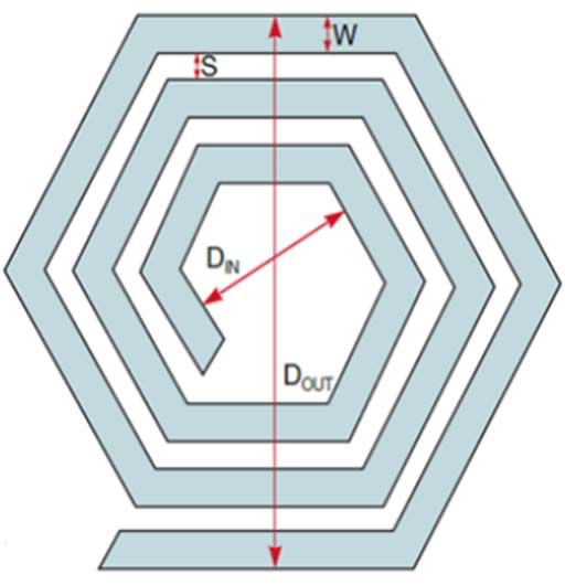
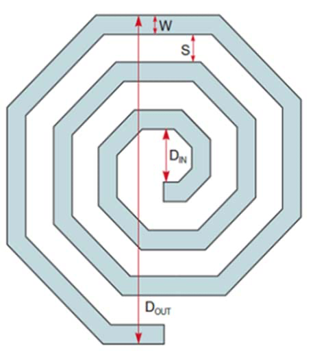
is (D out – D in )/(D out + D in ), and represents the fill ratio of the inductor – small values of correspond to hollow inductors (D out D in ), while large values correspond D in ). Different coil shapes are shown in Figure 1 to (D out and coil parameters are listed in Table 1.
is coupling coefficient and given by [2]
where is distance in millimeters between the inductors on two PCB layers. With multi-layer coils, there are more coupling factors. For 3 layers, there would be three coupling factors: , and . For 4 layers, there would be six coupling factors: , , , , and and so on. Equation (2) can be easily extended to calculate
Table 1: PCB coil parameters Symbol Parameter Electrical parameters L Total inductance R S DC Resistance C P Capacitance (parasitic) Physical parameters D OUT Outer diameter of inductor M Number of PCB Layers N Turns per layer W Trace width
S Trace spacing X ij PCB Layer Stack mm/ mils
| Geometric parameters of coil | |||
|---|---|---|---|
| r Coil fill ratio | - | ||
| DAVG Average diameter | mm/mils | ||
| ρ Geometric mean diameter | mm/mils | ||
| Copper Resistivity | 1.68×10⁻⁸ | ||
| (a) | (b) | l Coil length per layer | Ωm mm/mils |
Performance parameters of the application Q F X R Q factor Resonance frequency Resonance impedance Hz Ω Circuit components C T Tank capacitance F
inductance of these multi-layer coils.
is the resistivity of the conductor in Ω.m (5)
is the frequency in Hertz is the relative magnetic permeability of the conductor The parasitic capacitance for a multilayer coil can be calculated as given in [1]. The self-resonant frequency of the coil is given by,
number of parameters. Few of the physical parameters are fixed by the manufacturing process. Based on largely used variables in the design, a tradeoff matrix between the physical parameters is shown in Table 2 [11]. In addition to these dependencies, one can plot tradeoff graph with
Minimum required takes into account the vias to be placed at the center of the coil for connections, is given by
S = Via to Via spacing, and S = Via to Trace spacing
e
[5] H. M. Greenhouse, "Design of planar rectangular
microelectronic inductors", IEEE Trans. Parts, Hybrids, Packaging, vol. PHP-10, pp. 101-109, 1974 [6] J. Song, S. Kim, B. Bae, J. J. Kim, D. H. Jung and J.
Kim, "Design and analysis of magnetically coupled coil structures for PCB-to-active interposer wireless power transfer in 2.5D/3D-IC," 2014 IEEE Electrical Design of Advanced Packaging & Systems Symposium (EDAPS), Bangalore, 2014, pp. 1-4. [7] P. Meyer, P. Germano, M. Markovic and Y. Perriard,
"Design of a Contactless Energy-Transfer System for Desktop Peripherals," in IEEE Transactions on Industry Applications, vol. 47, no. 4, pp. 1643-1651, July-Aug. 2011 [8] LDC Reference Coils User’s Guide, 14 May 2015,
Texas Instruments. [9] LDC Sensor Design, March 2015, Texas Instruments. [10] Srinivasan, S., Chawda, P., Srikanth, P. A. M., Mac,
D., Mansour, M., & Perry, J. (2016). U.S. Patent No. 9,501,599. Washington, DC: U.S. Patent and Trademark Office. [11] Chawda, Pradeep Kumar, et al. "Method and
Apparatus for coil designer." U.S. Patent Application No. 15/053,816. [12] http://webench.ti.com/wb5/LDC/#/spirals [13] Asgaran, S. (2002, December). New accurate physics-
based closed-form expressions for compact modeling and design of on-chip spiral inductors. In Microelectronics, The 14th International Conference on 2002-ICM (pp. 247-250). IEEE.