⬇ Download Markdown  ·  ⬇ Download LaTeX  ·  ⬇ original  ·  view original

Interface-Engineered Giant Multistate Resistance Switching in Altermagnetic CrSb Multiferroic Tunnel Junctions arXiv:2607.15728v1 [cond-mat.mtrl-sci] 17 Jul 2026

Zhi Yan, ∗,†,‡ Yuwen Hua, † Yueting Li, † Xujin Zhang, † Jianhua Xiao, † and

ueting Li, Xujin Z Xiaohong Xu∗ ,†,‡

†School of Materials Science and Engineering & Key Laboratory of Magnetic Molecules and

Magnetic Information Materials of Ministry of Education, Shanxi Normal University,

Taiyuan 030031, China ‡Research Institute of Materials Science & Shanxi Key Laboratory of Advanced Magnetic

Materials and Devices, Shanxi Normal University, Taiyuan 030031, China

E-mail: [email protected]; [email protected]

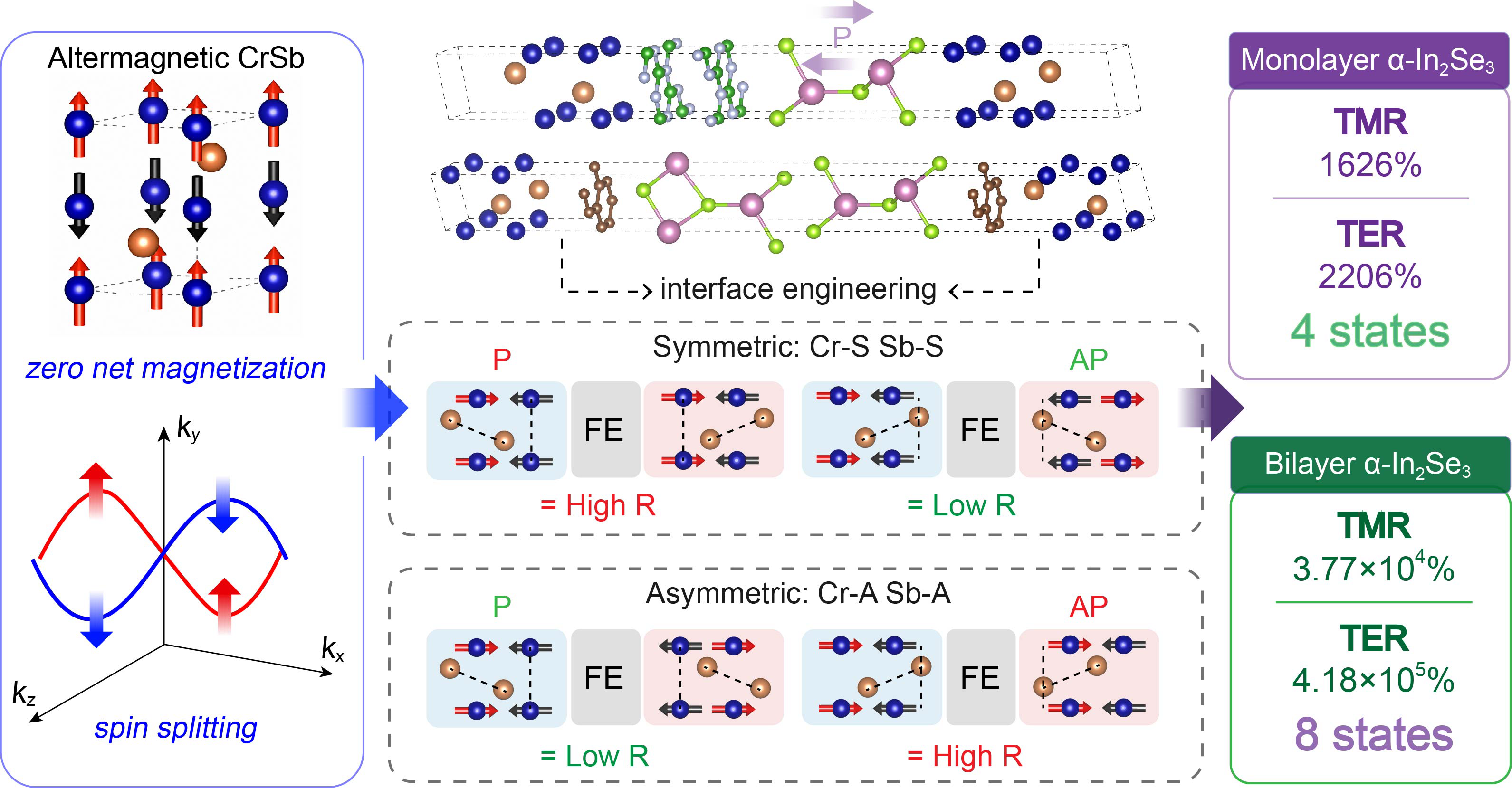
Abstract Altermagnets enable spin-split transport with- out stray magnetic fields, yet converting their momentum-dependent spin splitting into a strong tunnel-junction response requires interface-selected tunneling channels. Here, using density functional theory combined with nonequilibrium Green’s function calculations, we demonstrate giant multistate resistance switching in CrSb/α-In2 S e3 altermagnetic mul- tiferroic tunnel junctions. The response is governed not by the bulk spin splitting of CrSb alone, but by a symmetry-selected in- terfacial mechanism in which Cr/Sb termina- tions and h-BN or graphene insertion layers determine spin-channel matching, while fer- roelectric polarization reshapes the electro- static barrier. Symmetric and asymmetric terminations reverse the correspondence be- tween parallel/antiparallel N´eel-vector configu- rations and high-/low-resistance states, show- ing that the actual alignment of interfacial Cr moments selects the dominant tunneling channels. Monolayer-In2 S e3 junctions exhibit four nonvolatile resistance states, with tunnel- ing magnetoresistance (TMR) and tunneling electroresistance (TER) reaching 1626% and 2206%, respectively, and increasing to 9576% and 4144% upon Fermi-level shifting. Finite- bias calculations further reveal robust spin fil- tering and tunable spin-polarized currents. Ex- tending the barrier to bilayer In2 S e3 introduces interlayer polarization coupling, enabling eight resistance states with maximum TMR and TER values of 3.77 × 10⁴ % and 4.18 × 10⁵ %, respec- tively. These results establish interface sym- metry, spin-channel matching, and ferroelectric barrier reconstruction as design principles for stray-field-free multistate spintronic tunnel de- vices. Keywords: multiferroic tunnel junctions, al- termagnetism, spin-dependent tunneling, tun- neling magnetoresistance, tunneling electrore- sistance Introduction Spintronic devices exploit the electron spin de- gree of freedom for information storage and pro- cessing and are widely regarded as promising candidates for low-power information technolo- gies 1,2 . Among them, multiferroic tunnel junc- tions (MFTJs), consisting of two magnetic elec- trodes separated by a thin ferroelectric barrier, 1

are of particular interest because they combine tunneling magnetoresistance (TMR) and tun- neling electroresistance (TER) in a single de- vice platform 3 . By independently switching the ferroelectric polarization and the magnetic configuration of the electrodes, MFTJs can in principle realize multiple nonvolatile resistance states 4–11 . However, conventional MFTJs usu- ally rely on ferromagnetic electrodes, whose stray fields and relatively limited dynamical re- sponse can restrict device stability, scalability, and operation speed. Antiferromagnets avoid these drawbacks because of their compensated magnetization and ultrafast spin dynamics 12–14 , but their spin-degenerate electronic structures generally suppress spin-polarized tunneling and have limited their use in tunnel-junction de- vices 15,16 . Thus, an outstanding challenge is to realize strong spin-selective tunneling in a magnetic system that remains free of net mag- netization. Altermagnets provide a promising route to address this challenge. Although they pos- sess compensated collinear magnetic order, the opposite-spin sublattices are connected by ro- tation, mirror, glide, or screw symmetries rather than by inversion or simple transla- tion 17,18 . This symmetry structure produces momentum-dependent spin splitting in the absence of net magnetization, with charac- teristic d-, g-, or i-wave forms 19–22 . Con- sequently, altermagnets combine the stray- field-free character of antiferromagnets with spin-selective transport features usually asso- ciated with ferromagnets 19–21,23,24 . A variety of time-reversal-symmetry-breaking responses have been predicted or observed in altermag- nets, including anomalous Hall and Nernst ef- fects, spin-split torques, and tunneling mag- netoresistance 17,22,25–30 . In particular, large TMR has been predicted in tunnel junctions with altermagnetic electrodes when the relative orientation of the N´eel vectors is varied 31–33 . Experimentally, spin-split altermagnetic band structures have been resolved in CrSb, MnTe, and KV2 S e2 O 34–36 . Among these candidates, metallic CrSb is especially attractive for tunnel- junction applications because it combines a high N´eel temperature of approximately 700 K with a large experimentally observed spin split- ting of 0.93 eV 37 . These properties make CrSb a natural elec- trode candidate for altermagnetic MFTJs. Once a ferroelectric barrier is introduced, how- ever, the resistance response is no longer de- termined solely by the N´eel-vector configura- tion, the magnitude of the altermagnetic spin splitting, or the direction of ferroelectric po- larization. At the atomic scale, the electrode termination, barrier composition, and inter- facial insertion geometry can modify orbital hybridization, local electrostatic potential, and spin-resolved tunneling channels, thereby af- fecting both TMR and TER. This interfacial sensitivity is particularly important for alter- magnetic junctions, because the spin splitting is strongly momentum dependent and the ver- tical tunneling current is dominated by selected regions of the two-dimensional Brillouin zone. Therefore, the key issue is not simply whether CrSb can generate a large TMR, but how the interface symmetry selects the momentum- and spin-resolved channels that convert the bulk al- termagnetic spin splitting into a measurable tunnel-junction response. In this sense, in- terface termination, spin-channel matching, and ferroelectric barrier reshaping should be treated as coupled microscopic degrees of free- dom rather than as separate structural details. Here, we investigate interface-dependent mul- tiferroic transport in CrSb/α-In2 S e3 - based altermagnetic MFTJs using first-principles calculations combined with nonequilibrium Green’s function methods. In contrast to previous CrSb-based altermagnetic tunnel- junction studies that mainly exploited N´eel- vector-dependent spin splitting or ferroelectric- polarization switching, the present work focuses on how atomic-scale interface symmetry se- lects the active tunneling channels and couples them to ferroelectric barrier reconstruction. We consider h-BN, graphene, and ferroelectric α-In2 S e3 as barrier or insertion components and construct a series of junctions with differ- ent barrier configurations and CrSb termina- tions. Our results reveal a symmetry-selected interface-termination–spin-channel-matching– ferroelectric-barrier-reshaping mechanism for 2

Figure 1: (a) Atomic and spin configurations of CrSb, where the opposite spin sublattices are connected by rotation and mirror operations. (b) High-symmetry k-paths and three-dimensional Brillouin zone with colored nodal planes of CrSb. (c) and (d) Band structures of CrSb along different k-paths. (e–g) Schematic atomic structures of CrSb/In2 S e3 / CrSb tunnel junctions with a monolayer In2 S e3 barrier under different interface terminations: (e) Cr-termination, (f) Sb-termination, and (g) Cr-Sb-termination. In each panel, the upper and lower parts correspond to the symmetric and asymmetric interface configurations, respectively. The purple arrows denote the ferroelectric polarization direction PF E of the In2 S e3 barrier, while the red and blue arrows represent the opposite spin sublattices in the CrSb electrodes. The shaded regions highlight the interfacial atomic layers.(h) Schematic atomic structures of interlayer-inserted CrSb/In2 S e3 / CrSb tunnel junctions with Cr- terminated and Sb-terminated interfaces. The black rectangles mark the periodic unit cells of the left and right electrodes, denoted as Lead1 and Lead2, respectively. 3

multistate resistance switching. For monolayer- In2 S e3 barriers, Cr-terminated interfaces gen- erally support stronger spin-selective tunneling than Sb-terminated ones, while switching be- tween symmetric and asymmetric terminations provides an additional route to high- and low- resistance states. In contrast, bilayer-In2 S e3 barriers introduce interlayer ferroelectric po- larization coupling and give rise to a richer dependence on polarization configuration and insertion-layer composition, enabling additional resistance states and substantially enhanced re- sistance modulation. These findings identify in- terface symmetry as a controllable microscopic variable for engineering multistate transport in altermagnetic MFTJs and suggest CrSb-based heterostructures as potential candidates for stray-field-free nonvolatile spintronic memory devices. RESULTS AND DISCUS- SION Structural Models of the Multifer- roic Tunnel Junctions Hexagonal CrSb crystallizes in the NiAs-type structure with space group P 63 / mmc, as shown in Fig. 1(a). In this structure, each Cr atom is coordinated by six Sb atoms, and the magnetic moments of adjacent Cr layers are antiparal- lel along the z direction, forming an A-type antiferromagnetic (A-AFM) ground state 18,38 . The two opposite-spin sublattices are related by the spin-group symmetry operations [C2 ∥ Mc ] or C2 ∥ C6 cτ c /2 , where C2 denotes spin rever- sal, Mc is the mirror operation perpendicu- lar to the c axis, and C6 cτ c /2 represents a 60◦ rotation around the c axis combined with a half-unit-cell translation. These symmetry op- erations protect spin degeneracy on specific momentum planes while allowing momentum- dependent spin splitting away from them, giv- ing rise to the characteristic g-wave altermag- netic spin splitting in CrSb 37 . As illustrated in Fig. 1(b,d), the Γ-M-K-Γ path lies within the symmetry-protected planes and therefore remains spin degenerate [Fig. 1(d)], whereas pronounced spin splitting appears along the off-plane L-Γ-L′ path [Fig. 1(c)]. This split- ting mainly originates from exchange interac- tions rather than spin-orbit coupling and pro- vides the spin-selective electronic structure re- quired for altermagnetic tunneling 18,23 . These features make CrSb a suitable altermagnetic electrode for realizing spin-dependent tunneling in MFTJs. We use monolayer α-In2 S e3 as the ferroelec- tric barrier because it is a prototypical two- dimensional ferroelectric with robust out-of- plane polarization near room temperature. The monolayer consists of five atomic layers stacked in the Se-In-Se-In-Se sequence, and its ferro- electricity mainly originates from the vertical asymmetry of the internal In-Se bonds, which gives rise to a switchable electric dipole along the z direction 39,40 . This out-of-plane switch- able polarization provides the essential degree of freedom for realizing tunneling electroresis- tance and nonvolatile resistance switching in MFTJs. To verify that the altermagnetic char- acter of the electrodes is preserved after form- ing the heterostructure, we compared the total energies of ferromagnetic and A-AFM configu- rations for both polarization states of CrSb/α- In2 S e3 . The results show that the CrSb elec- trodes retain the A-AFM ground state in the presence of the ferroelectric barrier, as shown in Fig. S1(a,b). Thus, the CrSb/α-In2 S e3 het- erostructure provides the required magnetic and ferroelectric ingredients for constructing al- termagnetic MFTJs. We first investigated CrSb/α-In2 S e3 / CrSb multiferroic tunnel junctions with only a mono- layer α-In2 S e3 barrier. To further investigate the effects of interface chemistry and struc- tural symmetry, six representative interface configurations were considered, as shown in Fig. 1(e–g): Cr-S (Cr-symmetric), Cr-A (Cr- asymmetric), Sb-S (Sb-symmetric), Sb-A (Sb- asymmetric), Cr-Sb-S (Cr-Sb-symmetric), and Cr-Sb-A (Cr-Sb-asymmetric). Here, S and A denote whether the two electrode/barrier inter- faces are symmetric or asymmetric with respect to the barrier center. In the transport calcu- lations, the N´eel vector of the left CrSb elec- trode is kept fixed, while that of the right elec- 4

Figure 2: Schematic mechanism of interface-controlled multistate resistance switching in CrSb/α- In2 S e3 altermagnetic multiferroic tunnel junctions. (a) Device structure consisting of two CrSb altermagnetic electrodes, vacuum or atomically thin h-BN/graphene insertion layers, and an α- In2 S e3 ferroelectric barrier. The CrSb electrodes possess compensated altermagnetic order with zero net magnetization (M = 0), while the ferroelectric polarization of α-In2 S e3 can be reversed between PF E → and PF E ←. The Cr/Sb termination and insertion layers provide atomic-scale interface engineering knobs for tuning spin-dependent tunneling. (b) Resistance hierarchy under symmetric and asymmetric interface terminations for the two ferroelectric polarization states and the parallel (P) or antiparallel (AP) N´eel-vector configurations. The red and blue petal-like symbols represent interface-selected altermagnetic spin channels, and the tilted barrier profiles illustrate the polarization-dependent electrostatic potential. Thick solid arrows indicate favorable spin-channel matching and low-resistance states, whereas dashed arrows indicate suppressed tunneling and high- resistance states. For symmetric terminations, the P configuration gives high resistance and the AP configuration gives low resistance for both polarization directions. In contrast, asymmetric terminations reverse this correspondence. Therefore, the resistance state is governed by the actual alignment of interfacial Cr moments and the associated spin-channel matching, rather than by the nominal P/AP label alone. trode is set either parallel (P) or antiparallel (AP) to the left one. Together with the two opposite ferroelectric polarization states of α- In2 S e3 , this setup enables both TMR and TER to be evaluated within the same junction plat- form. The resulting model series provides a controlled framework for clarifying how alter- magnetic spin splitting, ferroelectric polariza- tion, barrier composition, and atomic-scale in- terface termination jointly determine multistate tunneling transport. Before discussing the calculated transport 5

Table 1: Spin-resolved transmission coefficients, TER, and tunneling magnetoresistance of different interfaces with a monolayer In2 S e3 barrier. Interface termination Polarization and Ratio P state AP state TMR T↑ T↓ Tt ot = T↑ + T↓ T↑ T↓ Tt ot = T↑ + T↓ Cr-S PF E ← 4.04 × 10− 2 6.21 × 10− 2 1.02 × 10− 1 2.06 × 10− 2 4.83 × 10− 2 6.89 × 10− 2 48.8% PF E → 3.08 × 10− 2 6.02 × 10− 3 3.68 × 10− 2 1.39 × 10− 2 4.07 × 10− 2 5.46 × 10− 2 48.5% TER 178.5% 26% Cr-A PF E ← 2.53 × 10− 2 2.51 × 10− 2 5.05 × 10− 2 9.13 × 10− 3 3.69 × 10− 2 4.60 × 10− 2 9.6% PF E → 1.68 × 10− 2 4.84 × 10− 2 6.57 × 10− 2 6.83 × 10− 2 1.62 × 10− 2 6.45 × 10− 2 1.8% TER 30.19% 40.1% Sb-S PF E ← 1.92 × 10− 2 2.66 × 10− 2 4.58 × 10− 2 1.53 × 10− 2 2.84 × 10− 2 4.37 × 10− 2 4.8% PF E → 2.49 × 10− 2 8.30 × 10− 3 3.32 × 10− 2 1.32 × 10− 2 3.07 × 10− 2 4.39 × 10− 2 31.9% TER 37.86% 0.3% Sb-A PF E ← 1.15 × 10− 2 1.90 × 10− 2 3.05 × 10− 2 1.19 × 10− 2 2.81 × 10− 2 4.00 × 10− 2 31.32% PF E → 1.61 × 10− 2 2.34 × 10− 2 3.97 × 10− 2 2.81 × 10− 2 1.18 × 10− 2 3.99 × 10− 2 0.56% TER 30.3% 0.2% Cr-Sb-S PF E ← 4.83 × 10− 2 1.76 × 10− 3 5.01 × 10− 2 8.19 × 10− 3 3.33 × 10− 2 4.15 × 10− 2 20.7% PF E → 3.95 × 10− 2 1.36 × 10− 3 4.08 × 10− 2 1.47 × 10− 2 1.59 × 10− 2 3.06 × 10− 2 33.3% TER 22.8% 35.6% Cr-Sb-A PF E ← 3.28 × 10− 2 8.30 × 10− 3 4.11 × 10− 2 2.19 × 10− 3 4.83 × 10− 2 5.05 × 10− 2 22.9% PF E → 2.23 × 10− 2 1.51 × 10− 2 3.74 × 10− 2 1.57 × 10− 3 4.80 × 10− 2 4.96 × 10− 2 32.6% TER 9.9% 1.8% properties, we first summarize the physical switching mechanism of the proposed altermag- netic MFTJs in Fig. 2. As shown in Fig. 2(a), the device consists of two CrSb altermag- netic electrodes, vacuum or atomically thin h- BN/graphene insertion layers, and an α-In2 S e3 ferroelectric barrier. The compensated alter- magnetic order of CrSb gives zero net magneti- zation (M = 0), while still providing spin-split electronic states for spin-selective tunneling. The α-In2 S e3 barrier supplies two reversible po- larization states, PF E → and PF E ←, which re- shape the electrostatic barrier profile and band alignment. Meanwhile, the Cr/Sb termination and insertion layers provide atomic-scale in- terface engineering knobs for tuning the spin- dependent interfacial potential and tunneling channels. The resulting switching mechanism is illus- trated in Fig. 2(b). The device contains two coupled switching degrees of freedom: the rela- tive N´eel-vector configuration of the two CrSb electrodes and the ferroelectric polarization di- rection of the α-In2 S e3 barrier. Switching be- tween the P and AP N´eel-vector configura- tions changes the spin-channel matching be- tween the two electrode/barrier interfaces and gives rise to TMR, whereas reversing the fer- roelectric polarization modifies the barrier pro- file and produces TER. More importantly, the high- and low-resistance states are not deter- mined by the nominal P/AP label alone, but by the actual alignment of the interfacial Cr moments. For symmetric terminations, the P configuration corresponds to antiparallel inter- facial Cr moments and therefore gives a high- resistance state, whereas the AP configuration produces parallel interfacial Cr moments and a low-resistance state. For asymmetric ter- minations, this correspondence is reversed, so that P becomes the low-resistance configuration and AP becomes the high-resistance configura- tion. This termination-induced inversion per- sists for both PF E ← and PF E →, while the polarization reversal changes the barrier asym- metry and hence the TER response. There- fore, Cr/Sb termination and h-BN or graphene insertion layers couple interfacial spin-channel matching with ferroelectric barrier reconstruc- tion, enabling interface-controlled multistate resistance switching in CrSb/α-In2 S e3 alter- magnetic MFTJs. 6

Table 2: Spin-dependent electron transmission coefficients T↑ and T↓ , TMR, and TER of CrSb- based MFTJs with a Cr-symmetric (Cr-S) interface and seven different barrier layers. Cr-S Barrier layer Polarization and Ratio P state AP state TMR T↑ T↓ Tt ot = T↑ + T↓ T↑ T↓ Tt ot = T↑ + T↓ h-BN/In2 S e3 PF E → 1.32 × 10− 3 1.15 × 10− 2 1.28 × 10− 2 2.19 × 10− 3 4.05 × 10− 2 4.27 × 10− 2 234% PF E ← 3.04 × 10− 3 7.42 × 10− 3 1.05 × 10− 2 1.76 × 10− 3 4.17 × 10− 3 5.93 × 10− 3 77% TER 22% 620% Gr/In2 S e3 PF E → 2.43 × 10− 3 9.97 × 10− 3 1.24 × 10− 2 2.79 × 10− 3 1.95 × 10− 3 4.74 × 10− 3 162% PF E ← 2.29 × 10− 3 1.03 × 10− 2 1.26 × 10− 2 2.46 × 10− 3 3.74 × 10− 3 6.20 × 10− 3 103% TER 1.6% 30.8% h-BN/In2 S e3 / h-BN PF E → 2.02 × 10− 5 4.19 × 10− 5 6.21 × 10− 5 1.56 × 10− 5 4.13 × 10− 4 4.29 × 10− 4 591% PF E ← 3.92 × 10− 5 1.91 × 10− 5 5.83 × 10− 5 5.06 × 10− 5 3.43 × 10− 4 3.94 × 10− 4 576% TER 6.5% 8.9% Gr/In2 S e3 / Gr PF E → 1.01 × 10− 3 1.43 × 10− 3 2.44 × 10− 3 3.35 × 10− 4 2.93 × 10− 3 3.27 × 10− 3 34% PF E ← 1.29 × 10− 3 1.13 × 10− 3 2.42 × 10− 3 3.21 × 10− 4 3.07 × 10− 3 3.39 × 10− 3 40.1% TER 0.8% 3.7% h-BN/In2 S e3 / Gr PF E → 3.16 × 10− 4 1.79 × 10− 3 2.11 × 10− 3 5.02 × 10− 4 2.03 × 10− 3 2.53 × 10− 3 20% PF E ← 2.77 × 10− 5 6.38 × 10− 5 9.15 × 10− 5 2.62 × 10− 5 8.36 × 10− 5 1.10 × 10− 4 20% TER 2206% 2200% 2·h-BN/In2 S e3 PF E → 2.76 × 10− 5 2.21 × 10− 5 4.97 × 10− 5 1.74 × 10− 5 8.41 × 10− 4 8.58 × 10− 4 1626% PF E ← 1.05 × 10− 4 1.18 × 10− 4 2.23 × 10− 4 1.15 × 10− 4 6.91 × 10− 4 8.06 × 10− 4 261% TER 349% 6.5% 2·Gr/In2 S e3 PF E → 1.02 × 10− 3 2.24 × 10− 3 3.26 × 10− 3 1.26 × 10− 3 8.58 × 10− 4 2.12 × 10− 3 53.8% PF E ← 1.07 × 10− 3 2.13 × 10− 3 3.20 × 10− 3 1.33 × 10− 3 1.07 × 10− 3 2.40 × 10− 3 33.3% TER 1.87% 13.2% The calculated spin-resolved transmission co- efficients listed in Table 1 show that, although ferroelectric polarization reversal can modu- late the interfacial transmission to some extent, both the tunneling magnetoresistance and tun- neling electroresistance remain relatively small in these junctions. Unlike layered van der Waals electrodes, CrSb is a non-van-der-Waals metal- lic crystal, whose surface dangling bonds may strongly hybridize with the electronic states of the ferroelectric barrier. Such direct con- tact can modify the interfacial wave-function overlap, introduce interface states, and perturb the local electrostatic environment of α-In2 S e3 , thereby weakening the spin-filtering effect and reducing the sensitivity of the tunneling con- ductance to ferroelectric polarization reversal. These results indicate that the direct CrSb/α- In2 S e3 interface is insufficient for achieving ef- ficient multiferroic tunneling modulation, thus motivating the introduction of atomically thin insertion layers to regulate the interfacial cou- pling. To regulate this direct interfacial coupling, we introduce h-BN and graphene (Gr) as atom- ically thin insertion layers between CrSb and α-In2 S e3 . Both materials are structurally com- patible with the hexagonal lattice. The opti- mized in-plane lattice constants are 2.50 ˚A for h-BN 41,42 , 2.46 ˚A for Gr 43 , 4.106 ˚A for mono- layer α-In2 S e3 44 , and 4.101 ˚A for CrSb. There- fore, the in-plane lattice constant of C rSb i s adopted for all junction models, with √ 3 × √ 3 supercells of h-BN and Gr matched to a 1 × 1 cell of α-In2 S e3 . In this design, h-BN serves as an electronically inert spacer to suppress exces- sive interfacial hybridization, whereas Gr pro- vides a more conductive insertion layer with dis- tinct screening and orbital-coupling character- istics. These two insertion layers therefore en- able the interfacial coupling to be tuned from a weakly hybridized insulating-spacer regime to 7

Figure 3: Spin-resolved projected density of states (PDOS) along the transport direction (z axis) of CrSb-based altermagnetic MFTJs with different interfaces under equilibrium conditions, together with the corresponding crystal structures of the central scattering regions. (a) P→ state of the Cr-S interface; (b) P← state of the Cr-A interface; (c) P→ state of the Sb-S interface; (d) P→ state of the Sb-A interface. The Fermi level is indicated by the white dashed line. a more electronically coupled regime, providing an effective interface-engineering route to en- hance the multiferroic tunneling response. Based on this design strategy, we con- struct seven representative barrier config- urations composed of h-BN, Gr, and α- In2 S e3 : (i) h-BN/In2 S e3 , (ii) Gr/In2 S e3 , (iii) h-BN/In2 S e3 / h-BN, (iv) Gr/In2 S e3 / Gr, (v) h- BN/In2 S e3 / Gr, (vi) 2·h-BN/In2 S e3 , and (vii) 2·Gr/In2 S e3 . Following the preceding analysis of interface configurations in the direct-contact CrSb/α-In2 S e3 / CrSb junctions, we select four representative terminations, namely Cr-S, Cr- A, Sb-S, and Sb-A, for the subsequent insertion- layer devices, in order to investigate the effects of terminal atoms and interfacial symmetry on multiferroic tunneling transport. We first op- timize the interfacial stacking of Gr and h-BN on both Cr- and Sb-terminated CrSb surfaces. As shown in Fig. S2(a,b), the energetically preferred configurations are the Cr/Sb-hollow stacking for Gr and the Cr/Sb-N stacking for h- BN. The optimized structures are then used to construct the two-probe MFTJ devices shown in Fig. 1(h). Interface-Controlled TMR and TER at Equilibrium We first evaluate the equilibrium TMR and TER of monolayer-In2 S e3 - based CrSb MFTJs with four CrSb interface terminations and seven barrier configurations. As summarized in Ta- ble 2 for the representative Cr-S interface and in Tables S1–S3 for the other terminations, the transport response depends sensitively on both the Cr/Sb termination and the barrier com- position. For monolayer-In2 S e3 barriers, Cr- terminated interfaces (Cr-S and Cr-A) gener- ally show stronger resistance modulation than Sb-terminated interfaces (Sb-S and Sb-A), in- 8

Figure 4: k∥ - resolved transmission coefficients in the two-dimensional Brillouin zone at the Fermi level for CrSb-based MFTJs with four interface terminations under different ferroelectric polariza- tion states of In2 S e3 and P/AP N´eel-vector configurations of CrSb. (a)(e) Cr-S interface; (b)(f) Cr-A interface; (c)(g) Sb-S interface; (d)(h) Sb-A interface. dicating that interfacial Cr atoms provide more favorable spin-channel matching for altermag- netic tunneling. This trend demonstrates that the resistance modulation is not determined by the ferroelectric barrier alone, but by the combined effect of interface termination and insertion-layer composition. To analyze the microscopic origin of the re- sistance contrast, we select representative junc- tions that give the largest TMR or TER for each interface termination. For the Cr-S in- terface, the maximum TMR reaches 1626% in the 2·h-BN/In2 S e3 barrier, while the max- imum TER reaches 2206% in the asymmet- ric h-BN/In2 S e3 / Gr barrier. For the Cr-A interface, the optimal TMR and TER are 575% and 1992%, respectively. In contrast, Sb-terminated interfaces show weaker modu- lation, with maximum TMR and TER values below 500%. These representative cases are used below to clarify how the local interfacial magnetic arrangement, spin-channel matching, and polarization-dependent barrier profile de- termine the high- and low-resistance states. The microscopic origin of the high- and low- resistance states can be understood from the spin-resolved real-space projected density of states (PDOS) in the central scattering region, plotted in the (E, z) plane in Fig. 3. For all four interface types, the spectral weight at the Fermi level is strongly suppressed inside the barrier region, confirming that transport occurs in the tunneling regime. More importantly, the inter- facial magnetic arrangement determines which spin channel maintains better spectral continu- ity across the junction. For the symmetric in- terfaces (Cr-S and Sb-S), the P alignment of the electrode N´eel vectors corresponds to an antiferromagnetic arrangement of the interfa- cial Cr moments, which suppresses tunneling at the Fermi level and produces a high-resistance state. When the right-electrode N´eel vector is switched to the AP configuration, the in- terfacial Cr moments become ferromagnetically aligned, leading to stronger spectral continu- ity across the barrier for the dominant spin 9

Figure 5: Transmission coefficient near the Fermi level of the MFTJ with P and AP configurations, and the corresponding TMR and TER ratios as a function of energy relative to the Fermi level (E − EF ) . The left vertical axis represents the transmittance, and the right vertical axis represents TMR (%) and TER (%). channel and hence a low-resistance state. For the asymmetric interfaces (Cr-A and Sb-A), the correspondence between the P/AP alignment and the interfacial Cr-moment arrangement is reversed, and the high- and low-conductance states are accordingly interchanged, as shown in Fig. 3(b,d). Therefore, the TMR is not de- termined simply by the nominal P or AP label, but by the actual magnetic alignment of the in- terfacial Cr moments and its matching with the spin-dependent tunneling channels. This picture is further supported by the k∥ - resolved transmission at the Fermi level in the two-dimensional Brillouin zone, as shown in Fig. 4. Figures 4(a)–(d) correspond to the junc- tions with the maximum TMR for the four in- terface terminations. For the symmetric inter- faces (Cr-S and Sb-S), transmission hot spots are concentrated mainly in the spin-down chan- nel of the low-resistance configuration, whereas they are strongly suppressed in the correspond- ing high-resistance state. This behavior indi- cates not only a large TMR but also a pro- nounced spin-filtering effect. The asymmetric interfaces exhibit the reversed trend, consis- tent with the reversed relation between P/AP alignment and interfacial Cr-moment arrange- ment. In addition, Figs. 4(e)–(h) show that reversing the ferroelectric polarization of α- In2 S e3 significantly redistributes the transmis- sion weight in momentum space. The clear change in the hot-spot distribution between P→ and P← demonstrates that the ferroelec- tric barrier does not merely shift the overall resistance, but actively reshapes the available tunneling channels. The momentum-resolved transmission therefore provides direct evidence for the coexistence of large TMR and TER in the proposed MFTJs under equilibrium condi- tions. Finally, we examine the energy dependence of the optimized CrSb-based MFTJs within the range from −0.5 to +0.5 eV relative to the Fermi level. As shown in Fig. 5, both the transmission and the resulting TMR/TER ra- tios exhibit strong energy dependence. For the Cr-S interface, the TMR reaches 9576% at −0.37 eV [Fig. 5(a)], while for the Cr- A interface the TER increases to 4144% at −0.06 eV [Fig. 5(e)]. These off-Fermi-level enhancements indicate that the multiferroic transport response is highly sensitive to the energy-dependent interfacial tunneling spec- trum. Therefore, the giant TMR and TER are not restricted to a single equilibrium en- ergy point, but can be further modulated when the effective transport window is shifted, for ex- ample by electrostatic gating, carrier doping, or finite-bias operation. This energy depen- dence suggests an additional route for control- 10

Figure 6: Current as a function of bias voltage for the CrSb/2·h-BN/In2 S e3 / CrSb multiferroic tunnel junction with four different interfaces; (a-b) Cr-S interface; (c-d) Cr-A interface; (e-f) Sb-S interface; (g-h) Sb-A interface. ling the spin- and polarization-dependent tun- neling characteristics of CrSb-based MFTJs. Spin-Polarized Transport under Nonequilibrium Conditions To examine whether the interface-controlled multiferroic response survives beyond equi- librium, we calculate the bias-dependent spin-resolved current, TMR, TER, and spin- injection efficiency (SIE) in the range from −0.5 to 0.5 V. The main text focuses on the CrSb/2·h-BN/In2 S e3 / CrSb junction, which ex- hibits the largest equilibrium TMR among the monolayer-In2 S e3 - based structures. Re- sults for the CrSb/h-BN/In2 S e3 / h-BN/CrSb and CrSb/h-BN/In2 S e3 / Gr/CrSb junctions are provided in Figs. S3–S6 of the Supporting In- formation. Figure 6 shows the calculated I–V curves of 11

Figure 7: TMR (panels a, d, g, j), TER (panels b, e, h, k), and SIE (panels c, f, i, l) as a function of bias voltage for the CrSb/2·h-BN/In2 S e3 / CrSb multiferroic tunnel junction with four different interfaces; (a-c) Cr-S interface; (d-f) Cr-A interface; (g-i) Sb-S interface; (j-l) Sb-A interface. the CrSb/2·h-BN/In2 S e3 / CrSb junction with four interface terminations. Overall, the magni- tude of the total current increases with increas- ing bias for most magnetic and ferroelectric states, consistent with the widening of the bias- induced transport window. Nevertheless, the current remains strongly dependent on interface termination, N´eel-vector alignment, and ferro- electric polarization. The spin-resolved cur- rents show clear spin asymmetry in most config- urations, indicating that spin-selective tunnel- ing persists under finite bias. This spin asym- metry is especially pronounced for the Cr-S in- terface, where one spin channel dominates the total current over a broad bias range. The I– V curves also exhibit bias-polarity asymmetry, particularly for polarization-reversed states, re- flecting the combined effect of the polar ferro- electric barrier and the asymmetric interfacial electrostatic potential. The corresponding TMR, TER, and SIE ra- tios are summarized in Fig. 7. Unlike the total current, the TMR and TER show pronounced nonmonotonic bias dependence, indicating that the resistance ratios are controlled by the over- lap between the bias window and the spin- or polarization-dependent transmission chan- nels. For the Cr-S interface, a large TMR is retained near equilibrium, reaching about 1626% for the P→ polarization state [Fig. 7(a)]. The TER response shows a stronger depen- dence on polarization-induced barrier asymme- try and can remain several hundred percent over a broad bias range for selected termina- tions, particularly Sb-S and Sb-A [Figs. 7(h,k)]. This behavior indicates that the optimal inter- face for TMR and TER need not be the same under finite bias. The additional finite-bias results in the Sup- porting Information show that the barrier com- position further modulates the balance between current amplitude, spin filtering, and ferro- electric resistance switching. The CrSb/h- BN/In2 S e3 / h-BN/CrSb junction exhibits sharp TMR peaks at selected bias voltages (Figs. S3 and S4), while the graphene-inserted CrSb/h- 12

Figure 8: Structural schematics of multiferroic tunnel junctions with bilayer In2 S e3 as the ferro- electric barrier, showing four different interface termination types and seven distinct barrier layer configurations. The periodic unit cells of the left and right electrodes are highlighted with black dashed rectangles. The arrows on the Cr atoms indicate the local magnetic moments. The z-axis is the transport direction, and periodicity is maintained within the xy-plane. BN/In2 S e3 / Gr/CrSb junction generally sup- ports larger current amplitudes and enhanced TER peaks (Figs. S5 and S6). These trends are consistent with the reduced effective tunnel- ing resistance and stronger interfacial electronic coupling introduced by the thinner spacer con- figuration or by graphene insertion. In addition to the resistance ratios, the finite- bias SIE provides useful information on spin selectivity. For the CrSb/2·h-BN/In2 S e3 / CrSb junction, the SIE remains sizable over a broad bias range for all four interface terminations [Figs. 7(c,f,i,l)]. This is consistent with the spin-resolved I–V curves in Fig. 6, where one spin channel often dominates the total current. Therefore, the spin-selective tunneling induced by the altermagnetic CrSb electrodes is not limited to equilibrium, but can survive under finite-bias operation. These nonequilibrium results demonstrate that CrSb-based altermagnetic MFTJs retain sizable TMR, TER, and spin-polarized current responses under finite bias. The bias voltage does not simply suppress the resistance ratios; instead, it reshapes the effective transport win- dow and can selectively enhance TMR or TER when favorable spin- or polarization-dependent transmission channels are sampled. The dis- tinct behaviors of different barrier configura- tions further show that interface insertion layers provide an effective means to balance current amplitude, spin filtering, and ferroelectric resis- tance modulation in altermagnetic multiferroic tunnel junctions. 13

Equilibrium Transport Properties Modulated by Bilayer In2 S e3 Bar- riers To further extend the multistate functionality of CrSb-based multiferroic tunnel junctions and explore the role of interlayer ferroelectric polar- ization coupling in spin-dependent tunneling, we replace the monolayer In2 S e3 barrier with bi- layer In2 S e3 . As shown in Fig. 8, bilayer In2 S e3 can host four stable polarization configurations, namely the up, down, head-to-head, and tail-to- tail states. When these four ferroelectric config- urations are combined with the parallel (P) and antiparallel (AP) alignments of the CrSb N´eel vectors, the junction can in principle generate eight nonvolatile resistance states. This pro- vides an additional degree of freedom for mul- tistate memory and electric/magnetic coopera- tive modulation. We first calculated the bilayer In2 S e3 - barrier tunnel junctions without insertion layers. The calculated spin-resolved equilibrium transmis- sion coefficients, together with the correspond- ing TMR and TER values, are summarized in Table S4. Compared with the monolayer In2 S e3 junctions, the bilayer In2 S e3 barrier ex- hibits larger TMR and TER, indicating that the additional ferroelectric layer provides stronger modulation of spin-dependent tunneling trans- port. However, the transport performance still strongly depends on the interface termination, suggesting that the direct CrSb/In2 S e3 contact continues to play an important role in spin- dependent tunneling. Therefore, it is necessary to further introduce h-BN and Gr insertion lay- ers to regulate the interfacial coupling. Based on this design concept, we construct bilayer-In2 S e3 - based CrSb MFTJs with four in- terface terminations, namely Cr-S, Cr-A, Sb- S, and Sb-A, consistent with the monolayer- barrier devices. In addition, h-BN and Gr are introduced as insertion layers to form seven representative composite barriers, denoted as h-BN/Gr, 2·h-BN, h-BN/h-BN, h-BN, 2·Gr, Gr/Gr, and Gr, respectively, as illustrated in Fig. 8. This model series enables a systematic comparison of how interface termination, bar- rier composition, and bilayer ferroelectric po- larization configuration affect the equilibrium TMR and TER under the same CrSb altermag- netic electrodes. Figures 9(a)–(d) show the equilibrium TMR of the bilayer-In2 S e3 - based CrSb MFTJs with four different interface terminations. The TMR exhibits a strong dependence on interface ter- mination, barrier composition, and ferroelectric polarization configuration. For most interface types, changing the bilayer polarization state leads to a sizable variation in TMR, indicat- ing that the interlayer polarization arrangement can effectively modify the spin-dependent tun- neling channels. Among all configurations con- sidered, the CrSb/Gr/bilayer-In2 S e3 / Gr/CrSb junction with the Sb-S interface shows the largest TMR, reaching 3.77 × 10⁴ % [Fig. 9(c)]. This result differs from the monolayer-barrier case, where Cr-terminated interfaces generally dominate, and indicates that bilayer polariza- tion configurations introduce an additional elec- trostatic degree of freedom that can overcome the simple termination trend. In this case, the combined effect of graphene insertion, Sb-S ter- mination, and bilayer polarization reshapes the band matching and spin-dependent transmis- sion across the barrier, strongly amplifying the conductance difference between the P and AP states. The TER enhancement induced by bilayer In2 S e3 is even more pronounced. Figures 9(e)– (h) present the TER values obtained by com- paring different pairs of ferroelectric polariza- tion states under the P and AP magnetic configurations for the four interface termina- tions. The TER generally reaches the order of 103 % in many configurations, and several cases are further enhanced to the order of 104 % or even 105 %. In particular, for the CrSb/2·h- BN/bilayer-In2 S e3 / CrSb junction with the Cr- S interface, the TER reaches a maximum value of 4.18 × 10⁵ % [Fig. 9(e)]. This ultrahigh TER indicates that different bilayer polarization con- figurations can lead to drastically different tun- neling conductances, providing a highly effec- tive route for resistance-state modulation. The large TER can be understood from the strong sensitivity of tunneling transport to the polarization-dependent potential land- 14

Figure 9: TMR and TER of the CrSb multiferroic tunnel junction with bilayer In2 S e3 under four different interface terminations, for seven different barrier layers. (a)(e) Cr-S interface; (b)(f) Cr-A interface; (c)(g) Sb-S interface; (d)(h) Sb-A interface. scape. Compared with monolayer In2 S e3 , bi- layer In2 S e3 provides not only two uniform po- larization states, but also head-to-head and tail- to-tail configurations with distinct internal elec- trostatic profiles. These polarization configura- tions can modify the effective barrier height, in- terfacial charge screening, and band alignment between the electrodes and the barrier. Conse- quently, the transmission probability can vary strongly among different polarization states, giving rise to much larger TER values than in the monolayer case. These results show that bi- layer ferroelectric barriers provide an effective strategy for increasing both the number of non- volatile resistance states and the magnitude of resistance modulation in CrSb-based altermag- netic MFTJs. CONCLUSIONS In summary, we have investigated CrSb-based altermagnetic MFTJs with different Cr/Sb ter- minations, insertion layers, and ferroelectric barrier configurations, and clarified the micro- scopic origin of their spin- and polarization- dependent tunneling. The large resistance modulation is not simply a consequence of the bulk altermagnetic spin splitting of CrSb or the ferroelectric polarization reversal of In2 S e3 , but arises from the coupling among symme- try selected interface termination, spin channel matching, and ferroelectric barrier reshaping. For monolayer-In2 S e3 barriers, Cr-terminated interfaces generally yield stronger resistance modulation than Sb-terminated ones, with rep- resentative TMR and TER values reaching 1626% and 2206%, respectively; moreover, sym- metric and asymmetric terminations induce an inversion of the P/AP resistance hierarchy by reconfiguring the dominant spin-resolved tun- neling channels. The insertion of h-BN or graphene further modifies the interfacial po- tential, orbital hybridization, and spin-channel matching, while energy-dependent transmission and finite-bias calculations show that the resis- tance contrast, spin filtering, and spin-polarized current can be tuned by shifting the effective transport window. Extending the barrier to bi- layer In2 S e3 introduces interlayer polarization coupling, increases the number of nonvolatile resistance states from four to eight, and gives maximum TMR and TER values of 3.77 × 10⁴ % and 4.18 × 10⁵ %, respectively. These re- sults identify interface symmetry, termination- dependent spin-channel matching, and ferro- 15

electric barrier reconstruction as coupled de- sign principles for stray-field-free, electrically switchable, multistate spintronic tunnel de- vices. COMPUTATIONAL METH- ODS All structural relaxations, total-energy calcu- lations, and electronic-structure calculations were performed within density functional the- ory (DFT) using the Vienna Ab initio Sim- ulation Package (VASP) 45 . The projector augmented-wave (PAW) method was used to describe the electron–ion interaction 46 , and the exchange–correlation functional was treated within the generalized gradient approxima- tion (GGA) using the Perdew–Burke–Ernzerhof (PBE) form 47 . Long-range van der Waals in- teractions were included using the DFT-D3 method. A plane-wave cutoff energy of 500 eV was adopted. For slab and periodic het- erostructure models, a vacuum region of 20 ˚A was introduced along the out-of-plane direc- tion to avoid spurious interactions between pe- riodic images. All atoms were fully relaxed until the total-energy convergence criterion reached 10− 6 eV and the residual forces were smaller than 0.01 eV/˚A. A Γ-centered 13 × 13 × 1 k- point mesh was used for structural optimiza- tion and total-energy calculations of the two- dimensional heterostructures, while a 12×12×8 mesh was used for bulk CrSb. We did not ap- ply an on-site Hubbard correction to CrSb be- cause the electronic structure calculated with U = 0 shows the best agreement with avail- able angle-resolved photoemission spectroscopy (ARPES) measurements 34,37 . Unless otherwise specified, spin-polarized calculations were per- formed within a collinear magnetic framework without spin–orbit coupling because the alter- magnetic spin splitting in CrSb is primarily exchange-driven. Electron transport properties were calcu- lated by combining DFT with nonequilibrium Green’s function (NEGF) theory, as imple- mented in the Nanodcal package 48,49 . In the self-consistent transport calculations, a double- ζ polarized basis set was used for the atomic orbitals 50 , the kinetic-energy cutoff was set to 80 Hartree, and the Hamiltonian convergence threshold was set to 10− 4 eV. The electronic temperature was fixed at 300 K through the Fermi–Dirac distribution. To ensure conver- gence of the transmission spectra and current, a 100 × 100 × 1 k-point mesh was employed for all CrSb-based MFTJ configurations. Within the NEGF–DFT formalism, the spin- polarized current Iσ and conductance Gσ are given by the Landauer–B¨uttiker expres- sions 51,52 Iσ = e h Tσ (E) [fL ( E) − fR ( E)] dE, (1) Gσ = e2 h Tσ (EF ), (2) where σ =↑, ↓ denotes the spin channel, e is the electron charge, h is Planck’s constant, Tσ (E) is the spin-resolved transmission coefficient, and fL ( E) and fR ( E) are the Fermi–Dirac distribu- tion functions of the left and right electrodes, respectively. The total current is I = I↑ + I↓ . (3) The spin-injection efficiency (SIE) is defined as SIE = I↑ − I↓ I↑ + I↓ . (4) At zero bias, the corresponding quantity can be evaluated from the transmission coefficients at the Fermi level. The tunneling magnetoresistance (TMR) at equilibrium is defined as 53 TMR = |GP − GA P| min{GP , GA P} × 100% = |TP − TA P| min{TP , TA P} × 100%, (5) where GP and GA P (or TP and TA P) denote the conductances (or total transmission coeffi- cients at the Fermi level) for the parallel and an- tiparallel N´eel-vector configurations of the two CrSb electrodes, respectively. Under a finite bias voltage V , the TMR is evaluated from the 16

magnitudes of the currents as TMR(V ) = | |IP ( V )| − |IA P( V )| | min{|IP ( V )|, |IA P( V )|} × 100%. (6) The tunneling electroresistance (TER) is de- fined by comparing the two opposite ferroelec- tric polarization states of the barrier 54,55 , TER = |G→ − G← | min{G→ , G← } × 100% = |T→ − T← | min{T→ , T← } × 100%, (7) where G→ and G← (or T→ and T← ) denote the conductances (or total transmission coefficients at the Fermi level) for the two opposite ferro- electric polarization states of the barrier under a fixed magnetic configuration. At a finite bias voltage V , the TER under a fixed magnetic con- figuration m (m = P or AP) is defined as TERm ( V ) = | |Im ,→( V )| − |Im ,←( V )| | min{|Im ,→( V )|, |Im ,←( V )|} ×100%. (8) Here, Im ,→ and Im ,← are the total currents for the two opposite polarization states under the same magnetic configuration m and applied bias. Acknowledgement This work was sup- ported by the National Natural Science Founda- tion of China Regional Innovation and Develop- ment Joint Fund Key Program (No. U24A6002) and the National Natural Science Foundation of China (No. 12304148). References (1) Rotjanapittayakul, W.; Pijitrojana, W.; (3) Fusil, S.; Garcia, V.; Barthelemy, A.; Bibes, M. Magnetoelectric Devices for Spintronics. Annu. Rev. Mater. Res. 2014, 44, 91. (4) Zhuravlev, M. Y.; Maekawa, S.; Tsym- bal, E. Y. Effect of spin-dependent screen- ing on tunneling electroresistance and tun- neling magnetoresistance in multiferroic tunnel junctions. Phys. Rev. B 2010, 81, 104419. (5) Yan, Z.; Zhang, X.; Xiao, J.; Fang, C.; Xu, X. Giant Nonvolatile Multistate Re- sistance with Fully Magnetically Con- trolled van der Waals Multiferroic Tunnel Junctions. Nano Lett. 2025, 25, 8473. (6) Yan, Z.; Qiao, D.; Lu, W.; Dong, X.; Xu, X. Magnetic order dependent gi- ant tunneling magnetoresistance and electroresistance in van der Waals antiferromagnetic-multiferroic tunnel junctions. Phys. Rev. B 2025, 111, 045404. (7) Garcia, V.; Bibes, M. Ferroelectric tunnel junctions for information storage and pro- cessing. Nat. Commun. 2014, 5, 4289. (8) Cao, Q.; L¨u, W.; Wang, X. R.; Guan, X.; Wang, L.; Yan, S.; Wu, T.; Wang, X. Non- volatile Multistates Memories for High- Density Data Storage. ACS Appl. Mater. Interfaces 2020, 12, 42449. (9) Wu, Y.; Zhang, D.; Zhang, Y.-N.; Deng, L.; Peng, B. Nonreciprocal and Nonvolatile Electric-Field Switching of Magnetism in van der Waals Heterostruc- ture Multiferroics. Nano Lett. 2024, 24, 5929–5936.

(1) Rotjanapittayakul, W.; Pijitrojana, W.; Archer, T.; Sanvito, S.; Prasongkit, J. Spin injection and magnetoresistance in MoS2 - based tunnel junctions using Fe3 S i Heusler alloy electrodes. Sci. Rep. 2018, 8, 4779. (2) Chappert, C.; Fert, A.; Van Dau, F. N. The emergence of spin electronics in data storage. Nature Mater. 2007, 6, 813. 5929–5936. (10) Yan, Z.; Xiao, J.; Yang, R.; Xu, X. Two-dimensional van der Waals multifer- roic tunnel junctions for multi-state, low- power spintronics: A review. Chin. Phys. B 2026, 35, 067304. (11) Yan, Z.; Yang, R.; Fang, C.; Lu, W.; Xu, X. Giant electrode effect on tunneling magnetoresistance and electroresistance in 17

van der Waals intrinsic multiferroic tunnel junctions using VS2 . Phys. Rev. B 2024, 109, 205409. (12) Baltz, V.; Manchon, A.; Tsoi, M.; Moriyama, T.; Ono, T.; Tserkovnyak, Y. Antiferromagnetic spintronics. Rev. Mod. Phys. 2018, 90, 015005. (13) Xiong, D.; Jiang, Y.; Shi, K.; Du, A.; Yao, Y.; Guo, Z.; Zhu, D.; Cao, K.; Peng, S.; Cai, W.; Zhu, D.; Zhao, W. An- tiferromagnetic spintronics: An overview and outlook. Fundam. Res. 2022, 2, 522. (14) Shao, D.-F.; Tsymbal, E. Y. Antiferro- magnetic tunnel junctions for spintronics. npj Spintronics 2024, 2, 13. (15) Baldrati, L.; Ross, A.; Niizeki, T.; Schneider, C.; Ramos, R.; Cramer, J.; Gomonay, O.; Filianina, M.; Savchenko, T.; Heinze, D.; Kleibert, A.; Saitoh, E.; Sinova, J.; Kl¨aui, M. Full angular dependence of the spin Hall and ordinary magnetoresistance in epitaxial antiferromagnetic NiO(001)/Pt thin films. Phys. Rev. B 2018, 98, 024422. (16) Fischer, J.; Gomonay, O.; Schlitz, R.; Ganzhorn, K.; Vlietstra, N.; Al- thammer, M.; Huebl, H.; Opel, M.; Gross, R.; Goennenwein, S. T. B.; Gepraegs, S. Spin Hall magnetoresistance in antiferromagnet/heavy-metal het- erostructures. Physical Review B 2018, 97, 014417. (17) Naka, M.; Hayami, S.; Kusunose, H.; Yanagi, Y.; Motome, Y.; Seo, H. Spin cur- rent generation in organic antiferromag- nets. Nat. Commun. 2019, 10, 4305. (18) ˇSmejkal, L.; Sinova, J.; Jungwirth, T. Be- yond Conventional Ferromagnetism and Antiferromagnetism: A Phase with Non- relativistic Spin and Crystal Rotation Symmetry. Phys. Rev. X 2022, 12, 031042. (19) Fernandes, R. M.; de Carvalho, V. S.; Birol, T.; Pereira, R. G. Topological tran- sition from nodal to nodeless Zeeman splitting in altermagnets. Phys. Rev. B 2024, 109, 024404. (20) Cheng, Q.; Sun, Q.-F. Orientation- dependent Josephson effect in spin- singlet superconductor/altermagnet/spin- triplet superconductor junctions. Phys. Rev. B 2024, 109, 024517. (21) Ghorashi, S. A. A.; Hughes, T. L.; Cano, J. Altermagnetic Routes to Majo- rana Modes in Zero Net Magnetization. Phys. Rev. Lett. 2024, 133, 106601. (22) Gonzalez Betancourt, R. D.; Zubac, J.; Gonzalez-Hernandez, R. J.; Geishen- dorf, K.; Soban, Z.; Springholz, G.; Olejnik, K.; Smejkal, L.; Sinova, J.; Jungwirth, T.; Goennenwein, S. T. B.; Thomas, A.; Reichlova, H.; Zelezny, J.; Kriegner, D. Spontaneous Anomalous Hall Effect Arising from an Unconventional Compensated Magnetic Phase in a Semi- conductor. Phys. Rev. Lett. 2023, 130, 036702. (23) ˇSmejkal, L.; Sinova, J.; Jungwirth, T. Emerging Research Landscape of Alter- magnetism. Phys. Rev. X 2022, 12, 040501. (24) Zhang, R.-W.; Cui, C.; Li, R.; Duan, J.; Li, L.; Yu, Z.-M.; Yao, Y. Predictable Gate-Field Control of Spin in Altermag- nets with Spin-Layer Coupling. Phys. Rev. Lett. 2024, 133, 056401. (25) Hariki, A.; Takahashi, Y.; Kuneˇs, J. X- ray magnetic circular dichroism in RuO2 . Phys. Rev. B 2024, 109, 094413. (26) Badura, A. et al. Observation of the anomalous Nernst effect in altermagnetic candidate Mn5 S i3 . Nat. Commun. 2025, 16, 7111. (27) Han, L. et al. Nonvolatile anomalous Nernst effect in Mn5 S i3 with a collinear 18

N´eel vector. Phys. Rev. Appl. 2025, 23, 044066. (28) Karube, S.; Tanaka, T.; Sugawara, D.; Kadoguchi, N.; Kohda, M.; Nitta, J. Observation of Spin-Splitter Torque in Collinear Antiferromagnetic RuO2 . Phys. Rev. Lett. 2022, 129, 137201. (29) Gonz´alez-Hern´andez, R.; ˇSmejkal, L.; V´yborn´y, K.; Yahagi, Y.; Sinova, J.; Jung- wirth, T.; ˇZelezn´y, J. Efficient Electri- cal Spin Splitter Based on Nonrelativistic Collinear Antiferromagnetism. Phys. Rev. Lett. 2021, 126, 127701. (30) Naka, M.; Motome, Y.; Seo, H. Perovskite as a spin current generator. Phys. Rev. B 2021, 103, 125114. (31) Zhang, L.; Ni, G.; He, J.; Gao, G. Above room temperature multiferroic tun- nel junction with the altermagnetic metal CrSb. Phys. Rev. B 2025, 112, 064401. (32) Samanta, K.; Jiang, Y.-Y.; Paudel, T. R.; Shao, D.-F.; Tsymbal, E. Y. Tunnel- ing magnetoresistance in magnetic tunnel junctions with a single ferromagnetic elec- trode. Phys. Rev. B 2024, 109, 174407. (33) Liu, F.; Zhang, Z.; Yuan, X.; Liu, Y.; Zhu, S.; Lu, Z.; Xiong, R. Giant tun- neling magnetoresistance in insulated al- termagnet/ferromagnet junctions induced by spin-dependent tunneling effect. Phys. Rev. B 2024, 110, 134437. (34) Yang, G. et al. Three-dimensional map- ping of the altermagnetic spin splitting in CrSb. Nat. Commun. 2025, 16, 1442. (35) Lee, S.; Lee, S.; Jung, S.; Jung, J.; Kim, D.; Lee, Y.; Seok, B.; Kim, J.; Park, B. G.; Smejkal, L.; Kang, C.- J.; Kim, C. Broken Kramers Degeneracy in Altermagnetic MnTe. Phys. Rev. Lett. 2024, 132, 036702. (36) Jiang, B. et al. A metallic room- temperature d-wave altermagnet. Nat. Phys. 2025, 21, 754–759. (37) Ding, J. et al. Large Band Splitting in g- Wave Altermagnet CrSb. Phys. Rev. Lett. 2024, 133, 206401. (38) Park, I. J.; Kwon, S.; Lake, R. K. Ef- fects of filling, strain, and electric field on the N´eel vector in antiferromagnetic CrSb. Phys. Rev. B 2020, 102, 224426. (39) Ding, W.; Zhu, J.; Wang, Z.; Gao, Y.; Xiao, D.; Gu, Y.; Zhang, Z.; Zhu, W. Pre- diction of Intrinsic Two-Dimensional Fer- roelectrics in In2 S e3 and Other III2 − VI3 van der Waals Materials. Nat. Commun. 2017, 8, 14956. (40) Yan, Z.; Li, Z.; Han, Y.; Qiao, Z.; Xu, X. Giant tunneling magnetoresistance and electroresistance in α-In2 S e3 - based van der Waals multiferroic tunnel junctions. Phys. Rev. B 2022, 105, 075423. (41) Liu, L.; Feng, Y. P.; Shen, Z. X. Structural and electronic properties of h-BN. Phys. Rev. B 2003, 68, 104102. (42) Yan, Z.; Xiao, J.; Zhang, X.; Fang, C.; Xu, X. Giant Tunneling Magnetore- sistance in Mn-and V-Intercalated Graphene/h-BN Based van der Waals Magnetic Tunnel Junctions. Adv. Funct. Mater. 2026, 36, e11719. (43) Dong, X.; Shen, X.; Sun, X.; Bai, Y.; Yan, Z.; Xu, X. Voltage-tunable giant nonvolatile multiple-state resistance in sliding-interlayer ferroelectric h-BN van der Waals multiferroic tunnel junction. Phys. Rev. B 2023, 108, 085427. (44) Jacobs-Gedrim, R. B.; Shanmugam, M.; Jain, N.; Durcan, C. A.; Murphy, M. T.; Murray, T. M.; Matyi, R. J.; Moore, R. L.; Yu, B. Extraordinary Photoresponse in Two-Dimensional In2 S e3 Nanosheets. ACS Nano 2013, 8, 514–521. (45) Kresse, G.; Furthm¨uller, J. Efficient it- erative schemes for ab initio total-energy calculations using a plane-wave basis set. Phys. Rev. B 1996, 54, 11169. 19

(46) Bl¨ochl, P. E. Projector augmented-wave method. Phys. Rev. B 1994, 50, 17953. (47) Perdew, J. P.; Burke, K.; Ernzer- hof, M. Generalized Gradient Approxima- tion Made Simple. Phys. Rev. Lett. 1996, 77, 3865–3868. (48) Taylor, J.; Guo, H.; Wang, J. Ab initio modeling of quantum transport properties of molecular electronic devices. Phys. Rev. B 2001, 63, 245407. (49) Taylor, J.; Guo, H.; Wang, J. ab initio modeling of open systems: Charge trans- fer, electron conduction, and molecular switching of a C6 0 device. Phys. Rev. B 2001, 63, 121104(R). (50) Soler, J. M.; Artacho, E.; Gale, J. D.; Garc´ıa, A.; Junquera, J.; Ordej´on, P.; S´anchez-Portal, D. The SIESTA method for ab initio order-N materials simulation. J. Phys.: Condens. Matter 2002, 14,

2745.
(51) Meir, Y.; Wingreen, N. S. Landauer for-
mula for the current through an interact-
ing electron region. Phys. Rev. Lett. 1992,
68, 2512.
(52) Datta, S. Electronic Transport in Meso-
scopic Systems; Cambridge University
Press: Cambridge, 1995.
(53) Yuasa, S.; Nagahama, T.; Fukushima, A.;
Suzuki, Y.; Ando, K. Giant room-
temperature magnetoresistance in single-
crystal Fe/MgO/Fe magnetic tunnel junc-
tions. Nat. Mater. 2004, 3, 868.
(54) Tao, L. L.; Wang, J. Ferroelectricity and
tunneling electroresistance effect driven by
asymmetric polar interfaces in all-oxide
ferroelectric tunnel junctions. Appl. Phys.
Lett. 2016, 108, 062903.
(55) Kang, L.; Jiang, P.; Hao, H.; Zhou, Y.;
Zheng, X.; Zhang, L.; Zeng, Z. Giant tun-
nel electroresistance in ferroelectric tun-
nel junctions with metal contacts to two-
dimensional ferroelectric materials. Phys.
Rev. B 2021, 103, 125414.
20

TOC Graphic
21