⬇ Download Markdown · ⬇ Download LaTeX · ⬇ original · view original
Yichi Zhang 1,2 , Hua Bai 1 , Lei Han 1 , Jiankun Dai 1 , Chong Chen 1 , Shixuan Liang 1 , Yanzhang Cao 1 , Yingying Zhang 1 , Qian Wang 1 , Wenxuan Zhu 1 , Feng Pan 1 , Cheng Song 1, * 1 Key Laboratory of Advanced Materials (MOE), School of Materials Science and
Engineering, Tsinghua University, Beijing 100084, China. 2 Key Laboratory of Materials Modification by Laser, Ion and Electron Beams (MOE),
Dalian University of Technology, Dalian 116024, China.
Abstract
Due to nonrelativistic altermagnetic spin splitting effect (ASSE), altermagnets can
generate time-reversal-odd spin current and spin splitting torque (SST) with spin
polarization parallel to the Néel vector. Hence the effective manipulation of SST would
provide plenty of opportunities for designable spintronic devices, which remains
elusive. Here, the electrical control of SST is achieved in altermagnetic RuO 2 , based on
controllable Néel vector of RuO 2 and Néel vector-dependent generation of SST. We
demonstrate the current-induced switching of Néel vector via spin-orbit torque in RuO 2
films, according to the reversible polarity of electrical transport measurements and X-
ray magnetic linear dichroism (XMLD). The XMLD also unprecedentedly
demonstrates that Néel vector really exists in altermagnets. The switching of Néel
vector to the current direction and resultantly enhanced spin polarization parallel to the
Néel vector brings about stronger ASSE-induced spin current. Our findings not only
enrich the properties of altermagnets but also pave the way for high speed memories
and nano-oscillators with excellent controllability and efficiency.
1 Introduction
In the field of information storage, nonvolatile magnetic random-access memory
(MRAM) with high speed, high density and low dissipation plays a key role, and it requires efficient approaches, especially electrical ones, to recording data 1–4 . During the
past decades, great progress has been made in spintronics, and spin torques carrying
angular momentum has replaced current-induced Oersted field as the state of the art for writing technology 5–8 . The widely used spin torques include spin transfer torque (STT)
and spin-orbit torque (SOT), and corresponding STT-MRAM and SOT-MRAM possess the strengths of lower power consumption, higher storage density and better reliability 9– 11 . On one hand, the STT usually has higher spin torque efficiency due to nonrelativistic
ferromagnetic exchange splitting, but relevant devices are more fragile because of the writing current flowing directly through the magnetic tunneling junctions (MTJs) 12,13 .
On the other hand, for SOT-MRAM, although the writing current does not pass through
MTJs, the spin torque efficiency is restricted by spin-orbit coupling (SOC) of spin source materials 14,15 . Therefore, it will be much beneficial to the improvement of data
writing technique if the advantages of both STT and SOT can be combined together.
Recently, a new spin splitting torque (SST) related with nonrelativistic
altermagnetic spin splitting effect (ASSE) has been predicted theoretically in collinear
antiferromagnets with crystal and spin-rotation symmetries (Supplementary Materials Note S1), which are termed as altermagnets 16–21 . This SOC-independent ASSE is able
to generate nontrivial transverse spin current or out-of-plane polarized spin current with higher efficiency compared to other mechanisms, such as low crystal symmetry 22–24 .
Experimental evidence of SST has been reported in RuO 2 films with rutile crystal structure 25–27 . The SST exhibits controllable spin polarization with its direction parallel
to the Néel vector of the altermagnets, which can overcome the limitation of orthogonal
relation among charge current, spin polarization and spin current. Not only does RuO 2
possess desirable electrical conductivity despite being a metallic oxide, but it also has
relatively high Néel temperature above 300 K as well as feasible preparation techniques,
which are in favor of being applied in spintronic devices operating at room temperature 28–32 .
2 Most notably, the Néel vector of RuO 2 aligns along the [001] crystallographic axis,
and hence various behaviors related with SST can be observed in RuO 2 films with different crystallographic orientations 28,29 . For example, RuO 2 (101) films with tilted
Néel vector are not only able to generate SST with out-of-plane polarization in favor of field-free switching of the magnetization in adjacent magnetic layer 26,27 , but they can also be utilized for spin detection 33 . To extend the functionalities of altermagnetic spin
sources, SST is expected to be manipulated, which will be achieved once the Néel
vector can be controlled efficiently in altermagnets. Meanwhile, the effective control of
Néel vector is likely to change the band structure of altermagnets, which will also enrich the new physics of altermagnetic materials 34 . Taking into account the difficulty of using
extremely large magnetic field (usually dozens of Tesla) to overcome the anisotropic
field of RuO 2 , it is more applicable to adopt electrical approach as an alternative solution, which is also suitable for device integration 35,36 . In this work, we achieve the
effective manipulation of Néel vector to tune SST in altermagnetic RuO 2 via electrical
approach. More importantly, both (i) controllable Néel vector under electrical currents
and (ii) Néel vector-dependent generation of spin current and SST are two crucial
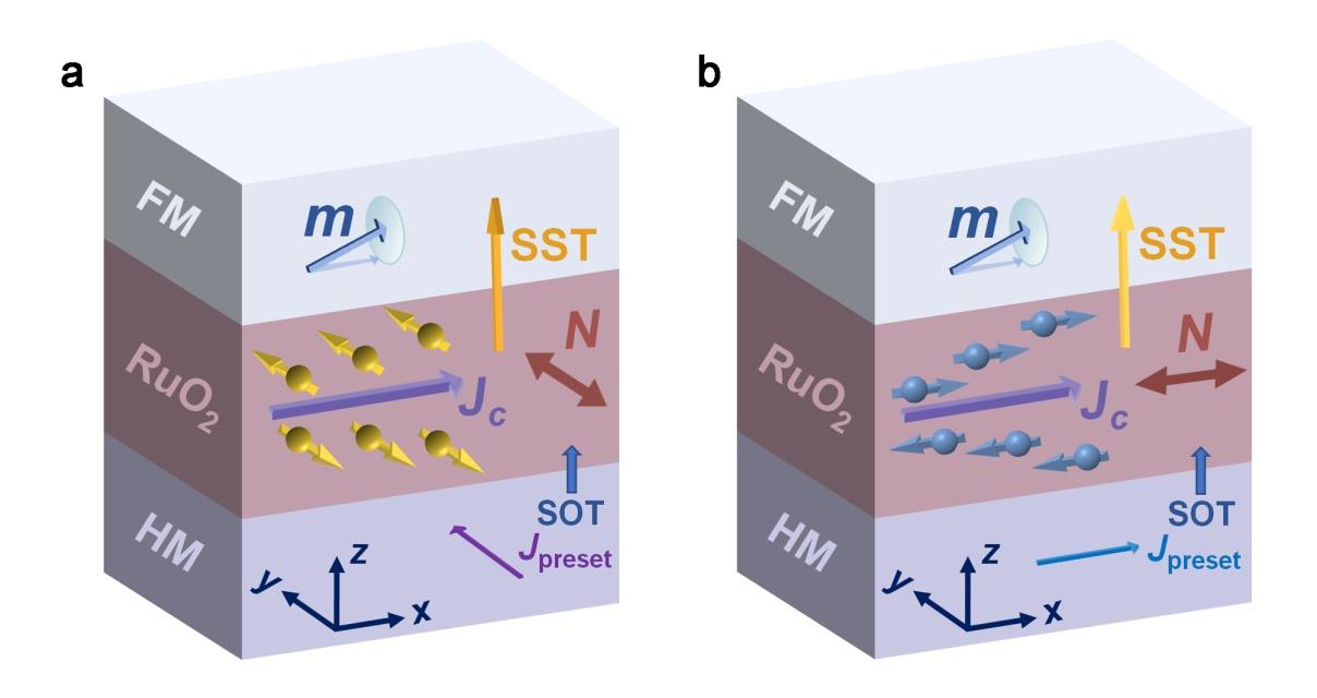
prerequisites to accomplish this task. As presented in Fig. 1a, a y-direction preset
current (J preset ) flowing inside heavy metal (HM) layer generates SOT and switches the
Néel vector (N) in RuO 2 layer to be along y-axis as well. The charge current (J C ) in
RuO 2 layer produces SST with spin polarization parallel to N, which is along y-axis (σ y ).
By comparison, if using another J preset along x-axis at first, we can align N along x-axis
and then obtain adjustable SST with x-direction spin polarization (σ x ) by applying J C ,
as displayed in Fig. 1b.
3
Fig. 1. Electrical manipulation of spin splitting torque in altermagnetic RuO 2 with
two operation schemes. a The y-direction J preset flowing in subjacent HM layer
generates SOT, leading to the alignment of N to be parallel with y-axis in RuO 2 layer,
and the charge current in RuO 2 layer produces SST with σ y . b The x-direction J preset
switches N to be along the x-direction, giving rise to tunable SST with σ x .
Results
Growth and fundamental characterizations of film samples
According to the physical picture of ASSE (Supplementary Materials Fig. S1),
RuO 2 (100) can generate SST by applying charge current while RuO 2 (110) cannot,
though the Néel vector lies in plane for both cases. To investigate SST manipulation in
altermagnetic RuO 2 , we need to achieve controllable Néel vector in RuO 2 films with
in-plane easy axis. Hence we deposited Pt/RuO 2 film samples on Al 2 O 3 (0001) and
MgO(100) substrates, respectively. The X-ray diffraction (XRD) patterns indicate that
RuO 2 has strong (100) and (110) texture in Al 2 O 3 /Pt/RuO 2 and MgO/Pt/RuO 2 samples
respectively, and they exhibit fine crystallization (Supplementary Materials Fig. S2).
The straight lines of magnetic field-dependent magnetization (M-H) curves measured
by superconducting quantum interference device (SQUID) at 300 K (Supplementary
Materials Fig. S3) can be accounted for by the diamagnetism of substrates, and there is
negligible net magnetization in Pt/RuO 2 (100) or Pt/RuO 2 (110). Besides, the 4 temperature-dependent magnetization (M-T) curves measured by SQUID reveal the
Néel temperature of RuO 2 films on Al 2 O 3 and MgO substrates to be 400~450 K
(Supplementary Materials Fig. S4). The Al 2 O 3 /Pt/RuO 2 and MgO/Pt/RuO 2 film samples
with desirable crystal quality and magnetization can be used for further depositing
comparable Py layers, which are also the basis for conducting following experiments
on various device samples (Supplementary Materials Fig. S5).
Current-induced Néel vector switching of RuO 2
First we investigate current-induced switching of Néel vector in altermagnetic RuO 2 by
electrical transport measurement at room temperature. We fabricated eight-terminal
devices of Pt(5 nm)/RuO 2 (15 nm) on Al 2 O 3 and MgO substrates. As shown in the inset
of Fig. 2a, each device has a pair of vertical (I write1 ) and horizontal (I write2 ) channels with
the width of 20 μm. After applying each writing current pulse with different magnitude
along one certain channel, the change of transverse Hall resistance (ΔR Hall ) is plotted in
Fig. 2a for RuO 2 (100) (red square) and RuO 2 (110) (blue diamond). When we increase
the magnitude of applied current pulses, no remarkable ΔR Hall signals can be observed until it reaches threshold value, corresponding with the current densities of 5.3×10 11 A m –2 and 4.8×10 11 A m –2 in Pt layer (J Pt ), for Pt/RuO 2 (100) and Pt/RuO 2 (110) samples respectively 27,37 . These critical values can be taken as reference to conduct the
following experiments. The slight discrepancy of critical switching current densities is
mainly caused by the different anisotropy when the films were deposited on different
substrates. Then we use critical switching currents to test each Pt/RuO 2 device for three
cycles: a group of five successive pulse currents with the same amplitude are applied
alternatively along the two orthogonal channels. Figure 2b displays ΔR Hall of RuO 2 (100)
(red square) and RuO 2 (110) (blue diamond) as a function of pulse numbers. For the two
Pt/RuO 2 devices, the obvious ΔR Hall is observed after applying the first pulse current,
and it increases gradually regarding the second to the fifth pulses. By comparison, no
apparent ΔR Hall signals can be detected in Pt or RuO 2 devices (Supplementary Materials
Note S4). Significantly, previous literature has reported that thermal artifacts could be observed in electrical Hall resistance measurements under specific circumstances 38 .
5 Hence to study the Joule heating caused by applied current pulses 39 , we meticulously
conducted both experiment measurement and finite element simulation, and the results
distinctly demonstrate that the temperature of device samples remains under the Néel
temperature from start to finish (Supplementary Materials Note S5). Therefore, the
recorded ΔR Hall of Pt/RuO 2 devices can be attributed to current-induced Néel vector
switching. The Hall resistance measurements preliminarily prove the in-plane Néel
vector switching with 90° in altermagnetic RuO 2 , where partial switching of domains is likely to exist here 40–43 .
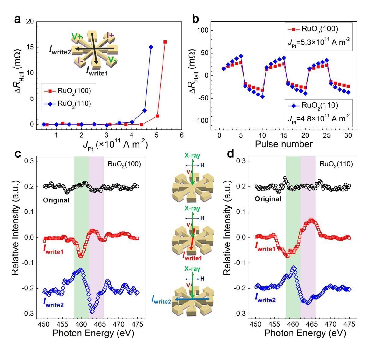
Fig. 2. Current-induced Néel vector switching in altermagnetic RuO 2 probed by
electrical transport and XMLD measurements. a ΔR Hall as a function of current
density in the Pt layer, with each data point being collected after applying one pulse
current. The inset shows the schematic of eight-terminal device for electric transport
measurement, where the read current and voltage paths are mutually perpendicular and
are aligned 45° to the two writing channels. b Pulse number dependence of ΔR Hall of
6 Pt/RuO 2 (100) (red square) and Pt/RuO 2 (110) (blue diamond) devices under critical
switching current densities. Ru M-edge XMLD results of Pt/RuO 2 devices for c
RuO 2 (100) and d RuO 2 (110). From top to bottom: before applying writing currents
(Original), after applying a group of five writing currents along vertical (I write1 ) channel
and along horizontal (I write2 ) channel.
To further verify the in-plane Néel vector switching in altermagnetic RuO 2 films,
we performed the measurement of Ru M-edge X-ray magnetic linear dichroism (XMLD)
at room temperature. By this synchrotron radiation test technique which is sensitive to
in-plane Néel vector, we can reveal the distribution of Néel vector in RuO 2 (100) and RuO 2 (110) and its dependence on writing currents 44–46 . Considering the compatibility with the size of detecting spot (80×80 μm 2 ) for XMLD measurement, we fabricated the
eight-terminal devices with 100 μm-wide writing channels here for Pt(5 nm)/RuO 2 (15
nm) in which the crystalline orientations of RuO 2 are (100) and (110). The detecting
light is focused on the intersection area of the device, and the signals of linearly
polarized X-ray absorption spectroscopy (XAS) are collected (Supplementary
Materials Fig. S11 and Fig. S12). The peak position of XAS curves near 462 eV
corresponds to the M 3 3p 3/2 binding energy of Ru element. The XMLD results presented
in Fig. 2c and Fig. 2d are obtained by the difference of linearly vertical (V) and
horizontal (H) polarized XAS signals.
Before applying writing currents, we collected XMLD signals of the initial state
of both devices. Due to non-epitaxial growth mode, twin crystal structure with different in-plane alignment of Néel vector exists in RuO 2 films 25 . Hence the in-plane Néel
vectors without uniaxial orientation cancel out each other, leading to no peaks or valleys
in XMLD results for the initial state of both switching devices, which is presented by
the (black circle) curves at the top of Fig. 2c and Fig. 2d. For each eight-terminal device,
writing currents are applied by following two schemes: a group of successive five pulse
currents flows through either the vertical channel (I write1 ) or the horizontal channel (I write2 ). The values of J Pt are 5.4×10 11 A m –2 and 4.9×10 11 A m –2 for Pt/RuO 2 (100) and
Pt/RuO 2 (110) devices, respectively. To ensure the repeatability of testing results, we
7 have measured sufficient switching devices after applying writing currents. Noticeably,
spikes appear in the XMLD signals after applying writing currents, as evidenced by the
representative peaks and valleys in middle (red square) and bottom (blue diamond)
curves in Fig. 2c and Fig. 2d. After I write1 flows through the vertical channel of
Pt/RuO 2 (100) and Pt/RuO 2 (110) devices, the XMLD curves undergo zero-negative-
positive-zero trace as photon energy increases, as displayed by two (red square) curves
in the middle of Fig. 2c and Fig. 2d. Meanwhile, after we applied I write2 to these devices,
the distinct XMLD signals can be seen in the two (blue diamond) curves at the bottom
of Fig. 2c and Fig. 2d. It is reasonable to deduce that after we used writing currents
which reached the threshold, the Néel vector is capable of being switched towards the
direction of charge current in Pt/RuO 2 devices. In contrast to their counterparts in the
middle, the two curves at the bottom of Fig. 2c and Fig. 2d reveal that the XMLD signals
exhibit a zero-positive-negative-zero tendency with increasing photon energy, which
indicates the reversed polarity of XMLD signals after we rotated the direction of writing
currents with in-plane 90°. Of note that there is a delay time from the application of
current pulses and the measurement of XAS (or XMLD) signals. We have prolonged
the delay time to make another test and observed the same phenomenon in XMLD
patterns, which proves the stability of XMLD measurement results (Supplementary
Materials Fig. S13). Therefore, the onefold orientation of Néel vector after applying
writing currents is determined by the direction of applied charge currents, which results
from SOT-induced Néel vector switching. The above XMLD measurements of Ru M-
edge support the current-induced switching of Néel vector with in-plane 90° in
altermagnetic RuO 2 , which is an important basis for manipulating SST because of the
close relation between SST and the state of Néel vector. The XMLD measurements also
unprecedentedly demonstrate that Néel vector really exists in the altermagnets, besides
the previous evidence deduced by transport measurements, such as the anomalous Hall effect and SST 25–27,35 .
Manipulation of spin splitting torque in RuO 2
To study the electrical control of spin splitting torque related to spin current generation
8 in altermagnetic RuO 2 , we fabricated Pt/RuO 2 (100)/Py and Pt/RuO 2 (110)/Py devices
for spin torque ferromagnetic resonance (ST-FMR) measurements, where the thickness
of each layer is indicated by Pt(5 nm)/RuO 2 (10 nm)/Py(15 nm). It is worth noting that
this well-established ST-FMR technique is particularly appropriate for detecting and analyzing spin currents with various spin polarizations (σ x , σ y and σ z ) 23,26,47,48 . Figure 3a
illustrates the setup of ST-FMR measurement to characterize the SST in Pt(5
nm)/RuO 2 (10 nm)/Py(15 nm) devices at room temperature. A radio-frequency (RF)
charge current flowing through the RuO 2 layer is converted into transverse spin current,
and then it is injected into the adjacent Py layer. According to the physical picture of
ASSE (Supplementary Materials Fig. S1), the spin-current generation is contributed by
ASSE together with spin Hall effect (SHE) in Pt/RuO 2 (100)/Py, while it is due solely
to SHE in Pt/RuO 2 (110)/Py. Under the applied magnetic field, the oscillating spin
current exerts spin torques on ferromagnetic Py layer leading to magnetization
precession. The external magnetic field is swept with φ H (angle between charge current
and applied magnetic field), which can be regarded the same as φ M (angle between
charge current and magnetization in Py) because of the relatively small in-plane
anisotropy of Py. Figure 3b displays a typical ST-FMR spectrum of Pt/RuO 2 (100)/Py
device after applying a group of writing currents (I write ) of 60 mA, and it is measured
with φ H = 45° under the excitation of 6 GHz and 19 dBm microwave current. As shown
in Fig. 3b (with more same type of data in Supplementary Materials Fig. S14), the
(black) dots are measured DC voltage data, and corresponding fitted V mix curve (green
one) can be decomposed into both symmetric (V S , blue one) and antisymmetric (V A , red
one) Lorentz line shapes. From the voltage signals, we can see that the amplitude of V A
(red line) is comparatively much larger than that of V S (blue line), for the Oersted field
plays a remarkable role in the former resulting from the shunting effect.
Each time after applying a group of five successive writing currents with the same
magnitude to Pt/RuO 2 /Py devices, we conducted an angle-dependent ST-FMR
measurement to characterize the SST in altermagnetic RuO 2 . The magnetic field was
applied in the plane of tested samples, and the angle between the Pt/RuO 2 /Py devices
and magnetic field was defined as φ H . We swept φ H with a step size of 15° under 6 GHz
9 and 19 dBm microwave currents. Of note is that RuO 2 (100) and RuO 2 (110) studied in
the present case can only generate in-plane spin polarizations (σ x and σ y ). Besides, V S
and V A are related with in-plane and out-of-plane current-induced spin torques
respectively (Supplementary Materials Table S1). Therefore, we are able to analyze spin
torques with in-plane polarization directions in Pt/RuO 2 (100)/Py device by
trigonometric function fitting, according to the acquired V S data. The fitting results after
applying I write = 60 mA and I write = 150 mA are presented in Fig 3c and Fig 3d, which
are below and above the critical switching current density, respectively. As depicted by
X (purple and orange) curves in Fig 3c and Fig 3d, prominent S
DL can be observed in Y the latter, while S
DL remains almost the same under the two circumstances.
10
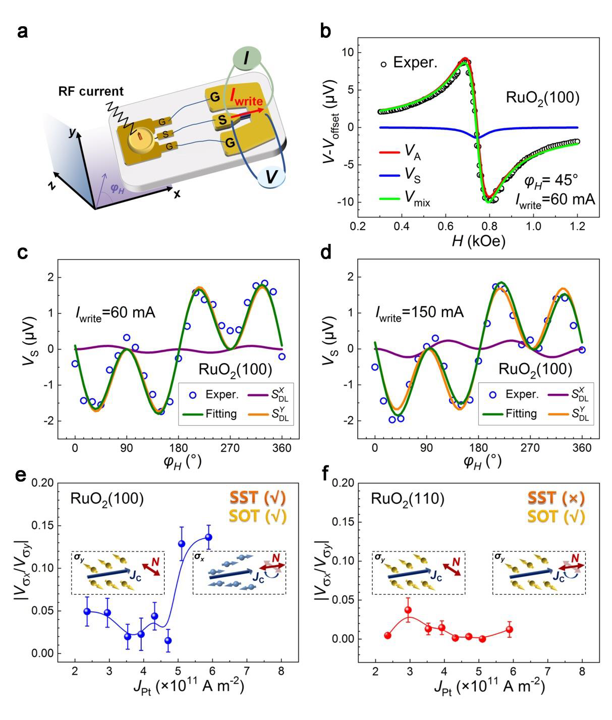
Fig. 3. Manipulation of spin splitting torque in altermagnetic RuO 2 characterized
by ST-FMR. a The measurement setup of ST-FMR. b A typical ST-FMR spectrum
consisted of antisymmetric (V A , red curve) and symmetric (V S , blue curve) signals under
φ H = 45° after applying writing currents of 60 mA. The analysis of spin torques with
various polarization directions by fitting the angle-dependent V S results after applying
writing currents of c 60 mA and d 150 mA. All data in panels b, c and d are obtained
by measuring Pt/RuO 2 (100)/Py device under 6 GHz and 19 dBm. The |V σx /V σy | data
points of e Pt/RuO 2 (100)/Py and f Pt/RuO 2 (110)/Py devices are displayed in terms of
different applied writing currents. The |V σx /V σy | indicates the ratio of dampinglike
torques with x-direction polarization (σ x ) to those with y-direction polarization (σ y ). The
11 data points with error bars in panels e and f are fitted by B-spline curves, and the insets
refer to the state of SST before and after Néel vector switching in Pt/RuO 2 (100)/Py and
Pt/RuO 2 (110)/Py devices.
Notably, both SST (by ASSE) and SOT (by SHE) give rise to σ y , but σ x can only
X Y be attributed to SST. Therefore, we extract the ratios of S
DL to S DL from the angle-
dependent measurements as |V σx /V σy | in terms of the writing currents. Correspondingly,
the data points of |V σx /V σy | connected by B-spline lines are presented in Fig. 3e and Fig.
3f for Pt/RuO 2 (100)/Py and Pt/RuO 2 (110)/Py, respectively. Taking into account the
multiple steps of data fitting with possible propagation of fitting errors, error bars are
also displayed accompanying the final data points in Fig. 3e and Fig. 3f. As the
magnitude of writing currents rises, the |V σx /V σy | for Pt/RuO 2 (100)/Py fluctuates within
a reasonable range, and then it increases abruptly at I write = 130 mA, as displayed in Fig. 3e. Under this situation, the corresponding writing current density is about 5.1×10 11 A m –2 , which reaches the threshold writing current density to trigger Néel vector
switching. This result is further verified by repeated experiment (Supplementary
Materials Fig. S15), whose critical value of current densities is also in accordance with
the previous results measured by SOT switching experiments. Hence this current-
induced Néel vector switching in RuO 2 layer leads to the alignment of Néel vector to
be along x-axis (being parallel to the direction of writing currents). Considering the
potential partial switching of Néel vector, further improvement of switching ratio of
domains will probably enhance the value of |V σx /V σy | to a larger extent. By contrast, Fig.
3f shows that there is no apparent enhancement for the σ x component in
Pt/RuO 2 (110)/Py as the writing currents increase, and typical angular-dependent ST-
FMR results of Pt/RuO 2 (110)/Py (Supplementary Materials Fig. S16) are also different
from those of Pt/RuO 2 (100)/Py shown in Fig 3c and Fig 3d.
Discussion
In view of the situation where the Néel vector lies in plane, RuO 2 (100) films have higher 12 spin torque efficiency than RuO 2 (110) films do because of the existence of SST in the
former, and the resultant spin torque conductivity surpasses that of many heavy metals
and topological insulators, which are potential candidates for efficient spin sources 10,14,25,49 . However, the spin polarization directions of SST are unable to be
changed in previous studies. To address this issue, a feasible solution is to manipulate
the Néel vector in altermagnets by electrical currents. Once the writing currents meet
the threshold, the SST can be tuned by applying charge currents in altermagnetic
RuO 2 (100) layer along x-axis: its spin polarization direction is parallel to the switched
Néel vector, which is shifted from σ y to σ x (Fig. 3e). After the Néel vector is switched
in RuO 2 (100), the proportion of σ x enhances but σ y still dominates, which can be
ascribed to conventional spin Hall effect. By comparison, no SST can be generated in
(110)-oriented RuO 2 by applied charge currents, according to the physical picture of
ASSE mechanism (Fig. 3f). Hence the generated transverse spin current comes entirely
from the conventional SHE depending on spin-orbit coupling, and the spin torques
regarding different in-plane coordinate axes cannot be tuned, which is irrelevant to the
Néel vector switching in RuO 2 (110).
It has been studied that magnetic moment-dependent spin torques can be produced
by magnetic SHE (e.g., in Mn 3 Sn) or antiferromagnetic SHE (e.g., in Mn 2 Au), abbreviated as MSHE or AFM-SHE respectively 24,50 . Therefore, altermagnetic
materials including RuO 2 with ASSE offers a new way to generate the spin torques
besides the above two counterparts. Meanwhile, the electric field control of Néel vector
in collinear antiferromagnet Mn 2 Au with AFM-SHE is also able to tune the Néel spinorbit torque (NSOT), which is different from the case in non-collinear Mn 3 Sn 50,51 .
Sharing the similarity of Néel vector-dependent generation of spin torques, the tunable
spin polarization of SST is parallel with the Néel vector in altermagnetic RuO 2 while
that of NSOT is perpendicular to the Néel vector in Mn 2 Au. Furthermore, compared to
Mn 2 Au relying on multi-step Rashba-like mechanism, our RuO 2 depends on
nonrelativistic altermagnetic spin splitting to generate spin current and spin splitting
torque with tunable polarization and higher efficiency.
In summary, we successfully achieve the electrical manipulation of altermagnetic
13 RuO 2 to tune the spin splitting torque, which is accomplished based on (i) controllable
Néel vector of RuO 2 and (ii) Néel vector-dependent generation of spin current and SST
due to ASSE. By applying electrical writing currents, the Néel vector in altermagnetic
RuO 2 with in-plane easy axis is switched by 90°. This current-induced switching is
evidenced by electrical transport measurements of transverse Hall resistance and it is
also manifested unambiguously by XMLD results in terms of the writing currents (and
their directions). The XMLD results also unprecedentedly demonstrate that Néel vector
really exists in altermagnets. Moreover, the spin polarizations of SST along different
coordinate axes are analyzed by the angular dependence of ST-FMR voltage signals,
and it proves distinctly that the SST can be tuned based on the control of Néel vector in
altermagnetic RuO 2 . The effective manipulation of spin splitting torque in
altermagnetic RuO 2 via a feasible electrical approach not only enriches the knowledge
of manipulating altermagnets with altermagnetic spin splitting effect, but it is also
beneficial to expanding the potential applications of altermagnetic spin sources with
controllable SST as the efficient writing technology in the field of information storage
involving MRAM.
Methods
Sample preparation
By DC magnetron sputtering method, two groups of Pt(5 nm)/RuO 2 (15 nm) film
samples were prepared on single-crystal Al 2 O 3 (0001) and MgO(100) substrates, and
single Pt(5 nm) and RuO 2 (15 nm) films were also deposited directly on the two
substrates. The Pt layers were deposited by sputtering Pt target with Ar flow of 20 at 773 K under a base pressure below 5×10 -5 Pa, and then they were annealed at 973 K for
1 hour. The RuO 2 layers were in-situ deposited by sputtering Ru target with Ar:O 2 flow
of 20:5 at 773 K. The deposition rates of Pt and RuO 2 films were 0.69 nm/min and 3.3
nm/min, respectively. For ST-FMR measurement, we deposited Pt(5 nm)/RuO 2 (10
nm)/Py(15 nm) film samples on Al 2 O 3 (0001) and MgO(100) substrates. After
depositing Pt and RuO 2 layers with the parameters introduced above, we in-situ
sputtered Py target with Ar flow of 20 at room temperature with the deposition rate of
14 1.33 nm/min. Also, the Pt(5 nm)/RuO 2 (10 nm)/Py(15 nm) film samples were in-situ
covered by 1 nm-thick Ru to prevent them from oxidation.
Sample characterization
Crystal quality and phase composition were analyzed by X-ray diffraction (XRD)
characterization utilizing a Rigaku Smartlab instrument with Cu-Kα radiation
(wavelength = 0.154 nm). The working voltage and working current were 40 kV and
150 mA, respectively. The scanning rate was 10°/min for each XRD pattern. Magnetic
field dependence of magnetization (M-H) curves were measured via a superconducting
quantum interference device (SQUID) from Quantum Design at room temperature.
Temperature dependence of magnetization (M-T) curves were measured via the same
SQUID instrument from 300 K to 600 K. Photographs of three kinds of devices were
taken by a Nikon ECLIPSE LV150NL optical microscope.
Fabrication of devices
By standard photolithography and Ar-ion milling techniques, the deposited Pt(5 nm),
RuO 2 (15 nm) and Pt(5 nm)/RuO 2 (15 nm) films on single-crystal Al 2 O 3 (0001) and
MgO(100) substrates were patterned into eight-terminal devices. The width of two
orthogonal writing channels was 20 μm (for electrical transport measurement) or 100
μm (for XAS and XMLD measurement), and the two diagonal detecting paths were 5
μm wide. By standard photolithography and Ar-ion milling techniques, the deposited
Pt(5 nm)/RuO 2 (10 nm)/Py(15 nm)/Ru(1 nm) films on Al 2 O 3 (0001) and MgO(100)
substrates were patterned into stripes whose length and width were 50 μm and 20 μm,
respectively. Then the Cr(10 nm)/Cu(80 nm) electrode was deposited on the stripes via
electron-beam evaporation method.
Electrical transport measurement
The two diagonal detecting paths of Pt(5 nm), RuO 2 (15 nm) and Pt(5 nm)/RuO 2 (15 nm)
devices were connected to a Keitheley 2400 current source offering a reading current
of 1 mA and a Keitheley 2182 nanovoltmeter recording transverse Hall voltage signals.
15 A Keysight 2901 power source was adopted to output current pulses, which was also
able to monitor the real-time resistance change of tested devices. A group of five
successive pulse currents with the same amplitude were applied along the horizontal
channel (red arrow I write1 in the inset of Fig. 2a), and then another group of writing
currents were applied along the vertical channel (blue arrow I write2 in the inset of Fig.
2a), which constituted a testing cycle. After applying each current pulse, the calculated
gap value of Hall resistance with respect to the initial value before applying this group
of current pulses is defined as the ΔR Hall XAS and XMLD measurements
XAS and XMLD measurements in total-electron-yield mode were carried out at the
beam line BL08U1A in the Shanghai Synchrotron Radiation Facility at 300 K. We used
this technique to probe into the in-plane distribution of Néel vector in altermagnetic
RuO 2 . The XMLD curves were the differences of linearly vertical (V) and horizontal
(H) polarized XAS signals. The detecting light was perpendicular to the sample plane, and the spot with the size of 80×80 μm 2 was focused on the intersection of eight-
terminal devices.
ST-FMR measurement
We adopted ST-FMR technique to characterize generated spin current and spin splitting
torque with different polarizations in altermagnetic RuO 2 . The sample holder was
connected to a Ceyear 1465F microwave source (0.1~40 GHz) via a bias-T which a
Keitheley 2182 nanovoltmeter was also linked to. External magnetic field was swept
along φ H (0° ≤ φ H ≤ 360°) with step size of 15°, and microwave current with 19 dBm
and 6 GHz was flowing through the stripe. Meanwhile, the direct current (DC) voltage
signals resulting from the anisotropic magnetoresistance (AMR) rectification of Py
were recorded by the nanovoltmeter, which were consisted of symmetric and
antisymmetric Lorentz line shapes, with the expression V = V S L S +V A L A . As for L A = ΔH(H-H res )/[(H-H res ) 2 +ΔH 2 ] and L S = (ΔH) 2 /[(H-H res ) 2 +ΔH 2 ], ΔH, H res and H represent
line width, resonance field and external magnetic field, respectively. For the spin
16 torques due to in-plane spin polarizations, the angular dependence of V S and V S could be described by the following equations 23,26 :
X Y V S = S DL sin 2 sin + S DL sin 2 cos (1)
X Y V A = A FL sin 2 sin + A FL sin 2 cos (2)
Y X X where S
DL and S DL were the coefficients of dampinglike (DL) torques, and A FL and Y were those of fieldlike (FL) torques, with A FL Y also including the A FL
contribution by Oersted field torque.
Finite element simulations
We utilized finite element simulations for analyzing the temperature rise due to applied
current pulses in Pt/RuO 2 devices. The simulated structures were Sub./Pt(5
nm)/RuO 2 (15 nm) where Sub. referred to single-crystal Al 2 O 3 (0001) and MgO(100)
substrates. Meanwhile, both writing channels of the simulated devices were 20 μm wide,
which was in line with the device structure in electrical transport measurement. For the
two Pt/RuO 2 devices, we applied a group of five 1 ms-wide current pulses with critical
value, and the interval between two successive pulses was 10 s. The thermal parameters of RuO 2 , including thermal conductivities (0.50 W cm -1 K -1 ) and specific heat capacities (56.42 J mol -1 K -1 ), were obtained from literature 52,53 , and those of Pt, Al 2 O 3 and MgO
were acquired directly from the build-in database of simulation software. The simulated
results (Supplementary Materials Fig. S10) could be classified as two categories: (i)
time-dependent temperature variation, and (ii) space-dependent temperature
distribution. For category (i), the monitoring space point was located at the center of
the Pt/RuO 2 switching devices (distance = 0 μm). For category (ii), the monitoring time
point was in the middle of one current pulse (t = 0.5 ms).
References
17 530-548 (2017).
nonvolatile magnetic random access memory. J. Appl. Phys. 85, 5828-5833 (1999).
magnetic tunnel junctions. Nat. Mater. 11, 64-68 (2012).
Rev. Mater. 4, 189-200 (2019).
Nat. Nanotechnol. 11, 231-241 (2016).
Nat. Phys. 11, 453-461 (2015).
(2015).
spin torque in antiferromagnetic devices. Nat. Phys. 14, 220-228 (2018).
Mater. 159, L1-L7 (1996).
Science 336, 555-558 (2012).
IEEE 104, 1449-1488 (2016).
Reliab. 52, 1848-1852 (2012).
potential applications. Prog. Mater. Sci. 118, 100761 (2021).
Materials, physics, and devices. Appl. Phys. Lett. 118, 120502 (2021).
nonrelativistic collinear antiferromagnetism. Phys. Rev. Lett. 126, 127701 (2021).
18
dependent spin splitting in centrosymmetric low-Z antiferromagnets. Phys. Rev. B
102, 014422 (2020).
B 103, 125114 (2021).
10, 4305 (2019).
Antiferromagnetism: A Phase with Nonrelativistic Spin and Crystal Rotation
Symmetry. Phys. Rev. X 12, 031042 (2022).
Altermagnetism. Phys. Rev. X 12, 040501 (2022).
reversal symmetry breaking and spontaneous Hall effect in collinear
antiferromagnets. Sci. Adv. 6, eaaz8809 (2020).
WTe 2 /ferromagnet bilayers. Nat. Phys. 13, 300-305 (2017).
20, 800-804 (2021).
RuO 2 . Phys. Rev. Lett. 128, 197202 (2022).
ruthenium dioxide. Nat. Electron. 5, 267-274 (2022).
RuO 2 . Phys. Rev. Lett. 129, 137201 (2022).
(2017).
resonant X-ray scattering. Phys. Rev. Lett. 122, 017202 (2019).
19
in uniquely strained RuO 2 films. Phys. Rev. Lett. 125, 147001 (2020).
Phys. Rev. 9, 041316 (2022).
Effect in Antiferromagnet RuO 2 . Phys. Rev. Lett. 130, 216701 (2023).
antiferromagnet. Sci. Adv. 10, eadn0479 (2024).
Electron. 5, 735-743 (2022).
magnetism: Materials, mechanisms, and performance. Prog. Mater. Sci. 87, 33-82
(2017).
MgO(001) by magnetron sputtering. Appl. Surf. Sci. 406, 212-217 (2017).
of Electrical Switching of the Antiferromagnetic Néel Vector. Phys. Rev. Lett. 123,
227203 (2019).
orbit torques and large anisotropic magnetoresistance. Nat. Commun. 9, 348
(2018).
antiferromagnetic moments in NiO. Sci. Rep. 8, 14167 (2018).
(2016).
heterostructure. Nat. Commun. 11, 5715 (2020).
topological surface state. Nat. Electron. 5, 574-578 (2022).
20 transition. Nat. Commun. 13, 1629 (2022).
Interface via Exchange Spring. Adv. Funct. Mater. 32, 2111653 (2022).
Pd/CoO/MgO(001). Phys. Rev. B 106, 214405 (2022).
resonance induced by the spin Hall effect. Phys. Rev. Lett. 106, 036601 (2011).
tungsten. Appl. Phys. Lett. 101, 122404 (2012).
Nature 511, 449-451 (2014).
antiferromagnet. Nature 565, 627-630 (2019).
antiferromagnet. Nat. Mater. 18, 931-935 (2019).
thermophysical and thermochemical properties of RuO 2 from 0 to 1000 K. J. Phys.
Chem. Solids 50, 429-434 (1989).
temperature thermal conductivity of RuO 2 by the photothermal deflection
technique. Appl. Phys. Lett. 94,131913 (2009).
Acknowledgments
Professor Wanjun Jiang and Le Zhao from Tsinghua University are greatly thanked for
the help with experiment. This work is supported by the National Key Research and
Development Program of China (Grant No. 2021YFB3601301) and the National
Natural Science Foundation of China (Grant No. 52225106, 12241404, T2394471, and
523B1007), and the Open Fund of the State Key Laboratory of Spintronics Devices and
Technologies (Grants No. SPL-2401). We acknowledge the beam line BL08U1A in
21 Shanghai Synchrotron Radiation Facility (SSRF) for the XAS and XMLD
measurements and the nanofabrication by Ultraviolet Maskless lithography machine
(model: Uv litho- AcA, tuotuo technology).
Author contributions
F.P and C.S. supervised the project. Y.Z. conceived the idea and designed the
experiments. Y.Z. conducted experiments, and H.B., L.H., J.D., C.C., S.L., Y.C., Y.Z.,
Q.W. and W.Z. helped with the experiments. Y.Z. wrote the original draft of the paper,
and H.B., L.H, and C.S. revised and edited the paper.
Competing interests
Authors declare that they have no competing interests.
Data availability
The data supporting the findings of this study are included in the paper and its
Supplementary Materials file. Further data sets are available from the corresponding
author on reasonable request.
22