⬇ Download Markdown · ⬇ Download LaTeX · ⬇ original · view original · CSV: table 1, table 2, table 3, table 4, table 5, table 6, table 7, table 8, table 9, table 10, table 11, table 12, table 13, table 14, table 15, table 16, table 17, table 18, table 19, table 20, table 21, table 22, table 23
Datasheet
| | Triaxis Hall Technology | HMI Non-Contacting Potentiometer |
|---|---|---|
| | Automotive Grade (AEC-Q100) | Joystick with Push |
| | Micro-power with Programmable Duty | Rotary with Push |
| Cycle | Linear (Long Stroke) | |
| | Selectable Digital Output | Top-Column Module |
| 16-bit Magnetic (XYZ) | Stalk Position/Function Sensor | |
| 16-bit Supply Voltage (V) | Center Stack | |
| 14-bit Temperature (T) | Shifter Position Sensor | |
| | At runtime programmable modes | Multimedia Rotary/Push Selector |
| Single Measurement | Knobs / Levers | |
| Burst Mode up to 2kHz (XYZ) | Body Control | |
| Wake-up On Change (WOC) Mode | Door handle & door lock | |
| | Programmable Measurement Range & | Mirror position |
| extended magnetic sensing range option | ||
| | On-chip magnetic calibration data allowing off-chip DSP to achieve maximum accuracy | 3. Description |
| | 8-bit measurement CRC Measurement Counter Selectable Bus Protocol – Slave node Up to 10MHz SPI or 1MHz I2 C 48-bit unique ID Number RoHS Compliant & Green Packages | The MLX90395 Triaxis Magnetic Node is a miniature monolithic sensor IC sensitive to the three orthogonal components of the flux density applied to the IC (i.e. BX , BY and BZ ) and to temperature. This allows the MLX90395 with the correct magnetic circuit to decode the absolute |
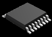
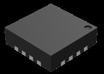
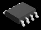
SOIC-8 TSSOP-16 QFN-16 A0 V DD A1 State Machine SDA/ MOSI Bias
RAM V X V Y V Z V V MUX Tria xis
® EEPROM Control SPI/ I2C Interface ADC G
V T Temp Compensation MS/ CS Interrupt Trigger Temp Sensor Oscillator Low Power Oscillator REVISION 6.0 - SEPTEMBER 15, 2020 3901090395 SCL/ SCLK MISO Wake-Up V SS HMI Non-Contacting Potentiometer Joystick with Push Rotary with Push Linear (Long Stroke) Top-Column Module Stalk Position/Function Sensor Center Stack Shifter Position Sensor Multimedia Rotary/Push Selector Knobs / Levers Body Control Door handle & door lock Mirror position
The MLX90395 Triaxis Magnetic Node is a miniature monolithic sensor IC sensitive to the three orthogonal components of the flux density applied to the IC (i.e. B X , B Y and B Z ) and to temperature. This allows the MLX90395 with the correct magnetic circuit to decode the absolute position of any moving magnet. It enables the design of novel generation of non-contacting position sensors that are frequently required for both automotive and industrial applications.
The MLX90395 selectable measurement data can be read over I 2 C or SPI bus. The sensor is runtime programmable and offers on-chip temperature compensation of the measured units. The selectable measurement duty cycle enables unsurpassed micro-power functionality. In this respect, the MLX90395 is the first true Software Defined Sensor: one IC, any magnetic sensing application. You define the function.

MLX90395 Triaxis® Magnetometer Node Datasheet
Note: Ordering code BAA-x0x: not recommended for new designs. Product Temperature Package Option Code Packing Form Definition MLX90395 MLX90395 MLX90395 MLX90395 MLX90395 MLX90395 MLX90395 MLX90395 MLX90395 MLX90395 MLX90395 MLX90395 K K K K K K K K K K K K DC GO LW DC GO LW DC GO LW DC GO LW BAA-000 BAA-000 BAA-000 BAA-100 BAA-100 BAA-100 BBA-001 BBA-001 BBA-001 BBA-101 BBA-101 BBA-101 RE RE RE RE RE RE RE RE RE RE RE RE Medium-Field Version (50mT) Medium-Field Version (50mT) Medium-Field Version (50mT) High-Field Version (120mT) High-Field Version (120mT) High-Field Version (120mT) Medium-Field Version (50mT) Medium-Field Version (50mT) Medium-Field Version (50mT) High-Field Version (120mT) High-Field Version (120mT) High-Field Version (120mT)
Temperature Code: Package Code:
Option Code - chip revision:
Option Code - application:
Packing Form:
Ordering Example:
K: from -40°C to 125°C “DC” for SOIC-8 package “GO” for TSSOP-16 package (dual die) “LW” for QFN-16 package (wettable flanks) Bxx-abc BAA: not recommended for new designs BBA: standard version Bxx-abc: a: Magnetic Sensing Range
0: Medium Field Version (50mT) 1: High Field Version (120mT) b: N/A c: SPI Filter
0: No filter (SPI frequency up to 10MHz) 1: 1MHz filter (SPI frequency up to 1MHz) “RE” for Reel
“DC”: 3000 pcs/reel “GO”: 4500 pcs/reel “LW”: 5000 pcs/reel “MLX90395KLW-BBA-101-RE” For a 120mT sensing range 3D Magnetic Node in QFN-16 package, delivered in Reel.
Table 1: Ordering information

REVISION 6.0 - SEPTEMBER 15, 2020 3901090395 Page 2 of 57

MLX90395 Triaxis® Magnetometer Node Datasheet
7.1. Pin Definition for SOIC-8 Package .................................................................................................... 8 7.2. Pin Definition for TSSOP-16 Package ............................................................................................... 8 7.3. Pin Definition for QFN-16 Package .................................................................................................. 9 8. Absolute Maximum Ratings .................................................................................................................... 10 9. Isolation Specification ............................................................................................................................. 10 10. General Description .............................................................................................................................. 11 11. General Electrical Specification ............................................................................................................ 12 12. Timing Specification ............................................................................................................................. 14 13. Temperature Specification ................................................................................................................... 15 14. Voltage Specification ............................................................................................................................ 15 15. Magnetic Field Requirements ............................................................................................................... 16
15.1. Medium-Field Variant (-0xx code) ............................................................................................... 16 15.2. High-Field Variant (-1xx code) ..................................................................................................... 16 16. Accuracy Specification .......................................................................................................................... 17
16.1. Medium-Field Variant (-0xx code) ............................................................................................... 17 16.2. High-Field Variant (-1xx code) ..................................................................................................... 18 17. Functional Description .......................................................................................................................... 19
17.1. Operating Modes ......................................................................................................................... 19 17.1.1. Single Measurement .............................................................................................................. 19 17.1.2. Burst Mode............................................................................................................................. 19 17.1.3. Wake-up on Change Mode .................................................................................................... 20 17.2. Flow Chart .................................................................................................................................... 21 17.3. Status Byte ................................................................................................................................... 22 17.3.1. Data Ready - DRDY ................................................................................................................. 22 17.3.2. Reset - RST .............................................................................................................................. 22

REVISION 6.0 - SEPTEMBER 15, 2020 3901090395 Page 3 of 57

MLX90395 Triaxis® Magnetometer Node Datasheet 17.3.3. Single Bit Error Corrected - SEC ............................................................................................. 22 17.3.4. Double Bit Error Detected - DED ........................................................................................... 22 17.3.5. Overflow - OVF ....................................................................................................................... 23 17.3.6. Communication Error - CE ..................................................................................................... 23 17.3.7. Measurement Counter .......................................................................................................... 23 17.4. Measurement CRC ....................................................................................................................... 24 17.4.1. CRC calculation ....................................................................................................................... 24 17.5. Commands ................................................................................................................................... 25 17.6. SPI Communication ...................................................................................................................... 25 17.6.1. Command implementation .................................................................................................... 27 17.6.2. SPI Timing Specification ......................................................................................................... 29 17.6.3. EMC filter (not re-programmable) - Not available in BAA version ........................................ 29 17.7. I 2 C Communication ...................................................................................................................... 30 17.7.1. Command Implementation .................................................................................................... 30 17.7.2. I 2 C Timing Specification ......................................................................................................... 32 18. Memory Structure and End-User Programmable Items ....................................................................... 33
18.1. NVRAM Endurance ...................................................................................................................... 33 18.2. Memory Structure ....................................................................................................................... 33 18.3. Register Map ................................................................................................................................ 34 18.3.1. Default NVRAM content ........................................................................................................ 36 18.4. Measurement Filters .................................................................................................................... 37 18.5. Communication and I 2 C Filters .................................................................................................... 38 18.6. Sensitivity ..................................................................................................................................... 39 18.7. Offset ............................................................................................................................................ 40 18.8. Burst and WOC Parameters ......................................................................................................... 40 18.9. Thermal Drift ................................................................................................................................ 40 18.10. External Trigger .......................................................................................................................... 41 18.11. NVRAM Lock (SPI mode) - Not available in BAA version ........................................................... 42 18.11.1. Temporary NVRAM Lock ...................................................................................................... 42 18.11.2. Permanent NVRAM Lock ..................................................................................................... 43 18.12. Other Controls ........................................................................................................................... 43 19. Recommended Application Diagrams .................................................................................................. 44
19.1. Wiring with the MLX90395 in SOIC-8/TSSOP-16 Package .......................................................... 44

REVISION 6.0 - SEPTEMBER 15, 2020 3901090395 Page 4 of 57

MLX90395 Triaxis® Magnetometer Node Datasheet 19.1.1. SPI Mode ................................................................................................................................ 44 19.1.2. I 2 C Mode ................................................................................................................................. 46 19.2. Wiring with the MLX90395 in QFN-16 Package .......................................................................... 47 19.2.1. SPI Mode ................................................................................................................................ 47 19.2.2. I 2 C Mode ................................................................................................................................. 49 20. Standard information regarding manufacturability of Melexis products with different soldering
processes ............................................................................................................................................... 50 21. ESD Precautions .................................................................................................................................... 50 22. Package Information ............................................................................................................................. 51
22.1. SOIC-8 Package ............................................................................................................................ 51 22.1.1. SOIC-8 - Package Dimensions ................................................................................................ 51 22.1.2. SOIC-8 - Pinout and Marking ................................................................................................. 52 22.1.3. SOIC-8 - Sensitive Spot Location ............................................................................................ 52 22.2. TSSOP-16 Package ........................................................................................................................ 53 22.2.1. TSSOP-16 - Package Dimensions ............................................................................................ 53 22.2.2. TSSOP-16 - Pinout and Marking ............................................................................................. 54 22.2.3. TSSOP-16 - Sensitive Spot Location ....................................................................................... 54 22.3. QFN-16 Package ........................................................................................................................... 55 22.3.1. QFN-16 - Package Dimensions and Sensitive Spot Location ................................................. 55 22.3.2. QFN-16 - Pinout and Marking (BAA version) ......................................................................... 55 22.3.3. QFN-16 - Pinout and Marking (BBA version) ......................................................................... 56 22.4. Package Thermal Performances .................................................................................................. 56 23. Contact ................................................................................................................................................. 57 24. Disclaimer ............................................................................................................................................. 57

REVISION 6.0 - SEPTEMBER 15, 2020 3901090395 Page 5 of 57

Datasheet
The MLX90395 is sensitive to the three (B X , B Y , B Z ) components of the flux density applied to the IC. This allows the MLX90395 with the correct off-chip signal processing to decode the absolute position of any moving magnet (e.g. rotary position from 0 to 360 Degrees, linear displacement, joystick… as shown in Figure 1). The flexibility resides in the runtime selection of measurement data and the application software in the external microcontroller, resulting in a true “Software-Defined Magnetic Sensor”.
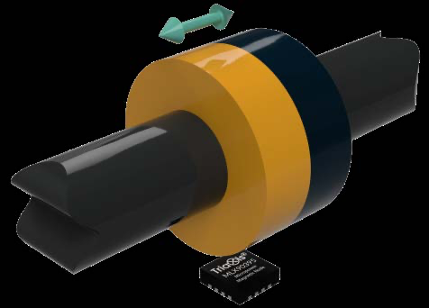
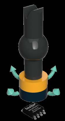
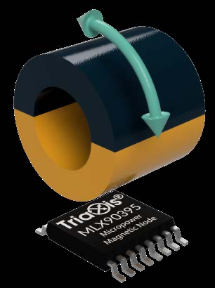
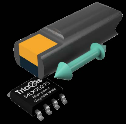
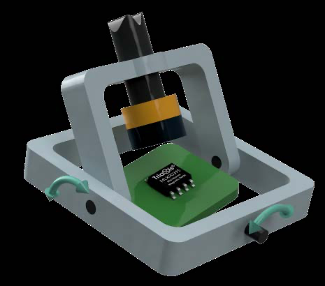
Figure 1: Magnetic Applications
As the MLX90395 has no on-board microcontroller, it lends itself well to applications requiring a concatenation of multiple sensors on the communication bus of a single microcontroller, allowing more cost-efficient and lean designs. Melexis’ Applications Engineers can support in the microcontroller computations.
Page 6 of 57

Datasheet V DD A0 A1 State Machine SDA/ MOSI EEPROM SCL/ SCLK Bias
RAM V V
® V X V Y V Z Control
SPI/ I2C Interface
V T Temp Compensation MISO MS/ CS Interrupt Trigger Temp Sensor Low Power Oscillator Oscillator V SS Wake-Up Figure 2: Block Diagram for the QFN-16 package A0 V DD State Machine Bias V X V Y V Z RAM EEPROM V V
®
ADC G Control SPI/ I2C Interface V T Temp Compensation
Temp Sensor Oscillator Low Power Oscillator Wake-Up SDA/ MOSI SCL/ SCLK MISO MS/ CS
Interrupt / Trigger V SS Figure 3: Block diagram for the SOIC-8 (single die) and TSSOP-16 (dual die) package
Page 7 of 57

Datasheet
Term Description Gauss (G), Tesla (T) TC ADC DAC LSB MSB DNL INL ASP DSP CDM HBM Units for the magnetic flux density:
| Term | Description | Term | Description | |||
|---|---|---|---|---|---|---|
| Gauss (G), Tesla (T) | Units for the magnetic flux density: 1mT = 10G | EMC | Electro-Magnetic Compatibility | |||
| TC | Temperature Coefficient (in ppm/°C) | FIR | Finite Impulse Response | |||
| ADC | Analog-to-Digital Converter | OSR | Over Sampling Rate | |||
| DAC | DAC | Digital-to-Analog Converter | Digital-to-Analog Converter | Digital-to-Analog Converter | PWL | Piece Wise Linear |
| LSB | LSB | Least Significant Bit | Least Significant Bit | Least Significant Bit | POR | Power On Reset |
| MSB | MSB | Most Significant Bit | Most Significant Bit | Most Significant Bit | SW | Software |
| DNL | DNL | Differential Non-Linearity | Differential Non-Linearity | Differential Non-Linearity | HW | Hardware |
| INL | INL | Integral Non-Linearity | Integral Non-Linearity | Integral Non-Linearity | IMC | Integrated Magnetic Concentrator |
| ASP | ASP | Analog Signal Processing | Analog Signal Processing | Analog Signal Processing | ROM | Read-only Memory |
| DSP | DSP | Digital Signal Processing | Digital Signal Processing | Digital Signal Processing | RAM | Random-access Memory |
| CDM | CDM | Charge Device Model | Charge Device Model | Charge Device Model | ESD | Electrostatic Discharge |
| HBM | HBM | Human Body Model | Human Body Model | Human Body Model | ||
| Table 2: Glossary of Terms 7. Pin Definitions 7.1. Pin Definition for SOIC-8 Package | Table 2: Glossary of Terms 7. Pin Definitions 7.1. Pin Definition for SOIC-8 Package | Table 2: Glossary of Terms 7. Pin Definitions 7.1. Pin Definition for SOIC-8 Package | Table 2: Glossary of Terms 7. Pin Definitions 7.1. Pin Definition for SOIC-8 Package | Table 2: Glossary of Terms 7. Pin Definitions 7.1. Pin Definition for SOIC-8 Package | Table 2: Glossary of Terms 7. Pin Definitions 7.1. Pin Definition for SOIC-8 Package | Table 2: Glossary of Terms 7. Pin Definitions 7.1. Pin Definition for SOIC-8 Package |
| Pin # | Name (I2 C) | Name (I2 C) | Name (SPI) | Description | Description | Description |
| 1 | SCL | SCL | SCLK | [I] Bus clock | [I] Bus clock | [I] Bus clock |
| 2 | SDA | SDA | MOSI | [I/O] Bus Data / SPI Master Out Slave In | [I/O] Bus Data / SPI Master Out Slave In | [I/O] Bus Data / SPI Master Out Slave In |
| 3 | Not Used | Not Used | MISO | [O] SPI Master In Slave Out | [O] SPI Master In Slave Out | [O] SPI Master In Slave Out |
| 4 | INT/TRG | INT/TRG | INT/TRG | [O or I] Interrupt / Trigger Pin (Programmable) | [O or I] Interrupt / Trigger Pin (Programmable) | [O or I] Interrupt / Trigger Pin (Programmable) |
| 5 | A0 | A0 | Not Used | [I] I2 C Address Pin 0 | [I] I2 C Address Pin 0 | [I] I2 C Address Pin 0 |
| 6 | V SS | V SS | V SS | [S] Ground | [S] Ground | [S] Ground |
| 7 | V DD | V DD | V DD | [S] Supply | [S] Supply | [S] Supply |
| 8 | MS | MS | /CS | [I] Mode Select / Chip Select | [I] Mode Select / Chip Select | [I] Mode Select / Chip Select |
| Table 3: SOIC-8 Pin Definitions and Descriptions For optimal EMC behaviour connect the unused pins (Not Used) to the Ground (See section 19.1). [I] stands for Input Pin, [O] stands for Output Pin and [S] stands for Supply Pin. 7.2. Pin Definition for TSSOP-16 Package | Table 3: SOIC-8 Pin Definitions and Descriptions For optimal EMC behaviour connect the unused pins (Not Used) to the Ground (See section 19.1). [I] stands for Input Pin, [O] stands for Output Pin and [S] stands for Supply Pin. 7.2. Pin Definition for TSSOP-16 Package | Table 3: SOIC-8 Pin Definitions and Descriptions For optimal EMC behaviour connect the unused pins (Not Used) to the Ground (See section 19.1). [I] stands for Input Pin, [O] stands for Output Pin and [S] stands for Supply Pin. 7.2. Pin Definition for TSSOP-16 Package | Table 3: SOIC-8 Pin Definitions and Descriptions For optimal EMC behaviour connect the unused pins (Not Used) to the Ground (See section 19.1). [I] stands for Input Pin, [O] stands for Output Pin and [S] stands for Supply Pin. 7.2. Pin Definition for TSSOP-16 Package | Table 3: SOIC-8 Pin Definitions and Descriptions For optimal EMC behaviour connect the unused pins (Not Used) to the Ground (See section 19.1). [I] stands for Input Pin, [O] stands for Output Pin and [S] stands for Supply Pin. 7.2. Pin Definition for TSSOP-16 Package | Table 3: SOIC-8 Pin Definitions and Descriptions For optimal EMC behaviour connect the unused pins (Not Used) to the Ground (See section 19.1). [I] stands for Input Pin, [O] stands for Output Pin and [S] stands for Supply Pin. 7.2. Pin Definition for TSSOP-16 Package | Table 3: SOIC-8 Pin Definitions and Descriptions For optimal EMC behaviour connect the unused pins (Not Used) to the Ground (See section 19.1). [I] stands for Input Pin, [O] stands for Output Pin and [S] stands for Supply Pin. 7.2. Pin Definition for TSSOP-16 Package |
| Pin # | Name (I2 C) | Name (I2 C) | Name (SPI) | Description | Description | Description |
| 1 | SCL1 | SCL1 | SCLK1 | [I] Bus clock | [I] Bus clock | [I] Bus clock |
| 2 | SDA1 | SDA1 | MOSI1 | [I/O] I2 C Data / SPI Master Out Slave In | [I/O] I2 C Data / SPI Master Out Slave In | [I/O] I2 C Data / SPI Master Out Slave In |
| 3 | Not Used | Not Used | MISO1 | [O] SPI Master In Slave Out | [O] SPI Master In Slave Out | [O] SPI Master In Slave Out |
| 4 | INT/TRG1 | INT/TRG1 | INT/TRG1 | [O or I] Interrupt / Trigger Pin (Programmable) | [O or I] Interrupt / Trigger Pin (Programmable) | [O or I] Interrupt / Trigger Pin (Programmable) |
| 5 | A02 | A02 | Not Used | [I] I2 C Address Pin 0 | [I] I2 C Address Pin 0 | [I] I2 C Address Pin 0 |
| 6 | V SS2 | V SS2 | V SS2 | [S] Ground | [S] Ground | [S] Ground |
| 7 | V DD2 | V DD2 | V DD2 | [S] Supply | [S] Supply | [S] Supply |
| 8 | MS2 | MS2 | /CS2 | [I] Mode Select / Chip Select | [I] Mode Select / Chip Select | [I] Mode Select / Chip Select |
Page 8 of 57

| Pin # | Name (I2 C) | Name (SPI) | Description |
|---|---|---|---|
| 10 | SDA2 | MOSI2 | [I/O] I2 C Data / SPI Master Out Slave In |
| 11 | Not Used | MISO2 | [O] SPI Master In Slave Out |
| 12 | INT/TRG2 | INT/TRG2 | [O or I] Interrupt / Trigger Pin (Programmable) |
| 13 | A01 | Not Used | [I] I2 C Address Pin 0 |
| 14 | V SS1 | V SS1 | [S] Ground |
| 15 | V DD1 | V DD1 | [S] Supply |
| 16 | MS1 | /CS1 | [I] Mode Select / Chip Select |
| Table 4: TSSOP-16 Pin Definitions and Descriptions For optimal EMC behaviour connect the unused pins (Not Used) to the Ground (See section 19.1). [I] stands for Input Pin, [O] stands for Output Pin and [S] stands for Supply Pin. 7.3. Pin Definition for QFN-16 Package | Table 4: TSSOP-16 Pin Definitions and Descriptions For optimal EMC behaviour connect the unused pins (Not Used) to the Ground (See section 19.1). [I] stands for Input Pin, [O] stands for Output Pin and [S] stands for Supply Pin. 7.3. Pin Definition for QFN-16 Package | Table 4: TSSOP-16 Pin Definitions and Descriptions For optimal EMC behaviour connect the unused pins (Not Used) to the Ground (See section 19.1). [I] stands for Input Pin, [O] stands for Output Pin and [S] stands for Supply Pin. 7.3. Pin Definition for QFN-16 Package | Table 4: TSSOP-16 Pin Definitions and Descriptions For optimal EMC behaviour connect the unused pins (Not Used) to the Ground (See section 19.1). [I] stands for Input Pin, [O] stands for Output Pin and [S] stands for Supply Pin. 7.3. Pin Definition for QFN-16 Package |
| Pin # | Name (I2 C) | Name (SPI) | Description |
| 1 | INT | INT | [O] Interrupt |
| 2 | MS | /CS | [I] Mode Select / Chip Select |
| 3 | SCL | SCLK | [I] Bus clock |
| 4 | Not Used | Not Used | Not Connected |
| 5 | SDA | MOSI | [I/O] I2 C Data / SPI Master Out Slave In |
| 6 | Not Used | MISO | [O] SPI Master In Slave Out |
| 7 | INT/TRG | INT/TRG | [O or I] Interrupt / Trigger Pin (Programmable) |
| 8 | Not Used | Not Used | Not Connected |
| 9 | Not Used | Not Used | Not Connected |
| 10 | Not Used | Not Used | Not Connected |
| 11 | A1 | Not Used | [I] I2 C Address Pin 1 |
| 12 | A0 | Not Used | [I] I2 C Address Pin 0 |
| 13 | V SS | V SS | [S] Ground |
| 14 | Not Used | Not Used | Not Connected |
| 15 | V DD | V DD | [S] Supply |
| 16 | Not Used | Not Used | Not Connected |
Page 9 of 57

Datasheet
| Parameter | Symbol | Min. | Typ. | Max. | Unit | Condition |
|---|---|---|---|---|---|---|
| Supply Voltage | V DDMAX | 4 | V | <48h | ||
| Reverse Voltage Protection | V DDREV | -0.3 | V | <48h | ||
| Positive Output Voltage | Vout | 4 | V | <48h Vout<V DD +0.3V | ||
| Negative Output Voltage | VoutREV | -0.3 | V | <48h | ||
| Positive Input Voltage(1) | Vin | 4 | V | <48h Vin<V DD +0.3V | ||
| Negative Input Voltage | VinREV | -0.3 | V | <48h | ||
| Operating Temperature | TAMB | -40 | +125 | °C | Refer to the qualification profile | |
| Junction Temperature | TJ | +150 | °C | |||
| Storage Temperature | TST | -40 | +150 | °C | Refer to the qualification profile | |
| Magnetic Flux Density | BMAX | -1 | +1 | T | ||
| ESD voltage, HBM | ESDHBM | -2 | +2 | kV | According AEC-Q100-002 DC and LW package code | |
| ESD voltage, CDM | ESDCDM | -750 | +750 | V | According AEC-Q100-011 DC and LW package code | |
| Table 6: Absolute Maximum Ratings Exceeding the absolute maximum ratings may cause permanent damage. Exposure to absolute maximum-rated conditions for extended periods may affect device reliability. 9. Isolation Specification Only valid for the package code GO, i.e. TSSOP-16 package (dual die). | Table 6: Absolute Maximum Ratings Exceeding the absolute maximum ratings may cause permanent damage. Exposure to absolute maximum-rated conditions for extended periods may affect device reliability. 9. Isolation Specification Only valid for the package code GO, i.e. TSSOP-16 package (dual die). | Table 6: Absolute Maximum Ratings Exceeding the absolute maximum ratings may cause permanent damage. Exposure to absolute maximum-rated conditions for extended periods may affect device reliability. 9. Isolation Specification Only valid for the package code GO, i.e. TSSOP-16 package (dual die). | Table 6: Absolute Maximum Ratings Exceeding the absolute maximum ratings may cause permanent damage. Exposure to absolute maximum-rated conditions for extended periods may affect device reliability. 9. Isolation Specification Only valid for the package code GO, i.e. TSSOP-16 package (dual die). | Table 6: Absolute Maximum Ratings Exceeding the absolute maximum ratings may cause permanent damage. Exposure to absolute maximum-rated conditions for extended periods may affect device reliability. 9. Isolation Specification Only valid for the package code GO, i.e. TSSOP-16 package (dual die). | Table 6: Absolute Maximum Ratings Exceeding the absolute maximum ratings may cause permanent damage. Exposure to absolute maximum-rated conditions for extended periods may affect device reliability. 9. Isolation Specification Only valid for the package code GO, i.e. TSSOP-16 package (dual die). | Table 6: Absolute Maximum Ratings Exceeding the absolute maximum ratings may cause permanent damage. Exposure to absolute maximum-rated conditions for extended periods may affect device reliability. 9. Isolation Specification Only valid for the package code GO, i.e. TSSOP-16 package (dual die). |
| Parameter | Symbol | Min. | Typ. | Max. | Unit | Condition |
Isolation Resistance R ISOL 4 Max. Unit Condition MΩ Between dies, measured between V SS 1 and V SS 2 with ±20V bias
Table 7: Isolation Specification 1 For shared [I/O] pin, maximum rating for output applies.
Page 10 of 57

Datasheet
As described on the block diagram the three vector components of the magnetic flux density (B X , B Y and B Z ) applied to the IC are sensed through the sensor front-end. The respective Hall signals (V X , V Y and V Z ) are generated at the Hall plates and amplified.
The analog front-end is based on a fully differential analog chain featuring the classic offset cancellation technique (Hall plate 4 Phases spinning and chopper-stabilized amplification).
The conditioned analog signals are converted through a sigma-delta ADC (19 bits) and provided to a DSP block for further processing. The DSP stage is a custom finite state machine whose primary function consists of signal conditioning of the raw XYZ signals: offset & sensitivity adjustment and thermal offset & sensitivity drift compensation using the calibrated on-board temperature sensor. The result of these computations are a predetermined transfer characteristic of the sensor for a fixed gain setting.
V DD A0 A1 State Machine SDA/ MOSI EEPROM SCL/ SCLK Bias
RAM
V X V Y V Z V V
MUX ®
Control SPI/ I2C Interface ADC G
V T Temp Compensation MISO MS/ CS Interrupt Trigger Temp Sensor Oscillator Low Power Oscillator Wake-Up V SS These 3D linear Hall measurements are made available to the communication bus master for readout. The supported communication protocols are both I 2 C and SPI, where the Triaxis Magnetic Node is a slave on the bus. Upon readback, it is then up to the microcontroller to process the measurement data – either in a vectorial or a scalar way – in order to achieve more complex position sensing functionality required by the application.
When processing data in a vectorial (or angular) way, all signal amplitude variations due to the sensitivity imperfections of the sensor, as well as the flux density degradation of the permanent magnet over temperature are cancelled out. The magnetic vectorial information is intrinsically self-compensated vs. flux density variations. This feature allows therefore an improved thermal accuracy vs. position sensors based on conventional 1D linear Hall sensors.
Another advantage of vectorial versus scalar signal processing is extended absolute position sensing range and higher linearity for Axial Parallel linear stroke position sensing applications.
In addition to the improved thermal accuracy, the realized position sensor features excellent linearity performances taking into account typical manufacturing tolerances (e.g. relative placement between the Hall IC and the magnet).
Page 11 of 57

Datasheet
General electrical specifications are valid for temperature range: -40 - 125°C, supply voltage range: 2.6/3.0 - 3.6V unless otherwise noted (condition).
| Parameter | Symbol | Min. | Typ. | Max. | Unit | Condition |
|---|---|---|---|---|---|---|
| Analog Supply Voltage | V DD | 2.6 | 3.3 | 3.6 | V | TA ≤ 90°C |
| Analog Supply Voltage | V DD | 3.0 | 3.3 | 3.6 | V | TA > 90°C |
| Supply Current(2) | Idd.convXY | 2.3 | 3 | mA | X-/Y-axis measurement | |
| Supply Current(2) | Idd.convZ | 3 | 4 | mA | Z-axis measurement | |
| Supply Current(2) | Idd.convT | 1.6 | 2 | mA | Temperature measurement | |
| Supply Current(2) | Idd.convV | 1.6 | 2 | mA | Voltage measurement | |
| Idle Current(2, 3) | Idd.idle | 1.4 1.4 | 9 20(5) | µA µA | TA ≤ 85°C TA within TAMB | |
| Standby Current(2, 4) | Idd.stby | 2.4 2.4 | 10 21(5) | µA µA | TA ≤ 85°C TA within TAMB | |
| Surge Current(2, 5) | Isurge | 25 | 250 | mA | Startup current, <3µs | |
| Power-On reset (rising) | VporLH | 1.45 | 1.52 | V | ||
| Power-On reset (falling) | VporLH | 1.3 | 1.39 | V | ||
| Input High Threshold(5) | VIH | 75 | %V DD | SDA/MOSI, SCL/SCLK | ||
| Input Low Threshold(5) | VIL | 25 | %V DD | SDA/MOSI, SCL/SCLK | ||
| Input Level Hysteresis(5) | VIHYST | 15 | 27 | %V DD | SDA/MOSI, SCL/SCLK | |
| Input High Threshold(5) | VIH | 70 | %V DD | INT/TRG, MS/CS | ||
| Input Low Threshold(5) | VIL | 20 | %V DD | INT/TRG, MS/CS | ||
| Input Level Hysteresis(5) | VIHYST | 17 | 22 | %V DD | INT/TRG, MS/CS | |
| Input Capacitance(5) | Cin | 5 | 30 | pF | ||
| Output Level High | VOH | 98 | %V DD | MISO, INT, INT/TRIG, SDA (Static, 1mA load) | ||
| Output Level Low | VOL | 2 | %V DD | MISO, INT, INT/TRIG, SDA (Static, 1mA load) | ||
| ON Resistance(5) | Rds.on | 4 | 6 | 9 | Ω | SDA |
| ON Resistance(5) | Rds.on | 13 | 20 | 27 | Ω | INT (NMOS and PMOS) |
| Output High Short Circuit Current(5) | IshortH | -60 | mA | Vout forced to 0V | ||
| Output Low Short Circuit Current(5) | IshortL | 110 | mA | Vout forced to V DD | ||
| 20 | nA | SDA | ||||
| Leakage Current(5) | Ileak | 25 0.1 | nA nA | INT MISO | ||
| 20 | nA | SCLK, MS/CS | ||||
| Main Oscillator Frequency | FOSC | 0.95 | 1 | 1.05 | MHz | TA = 35°C |
| Main Oscillator Thermal Drift | FOSC_TH | -5 | 5 | %FOSC | TA within TAMB | |
| Low Power Oscillator Frequency | FLPOSC | 48 | 50 | 52 | kHz | TA = 35°C |
| LP Oscillator Thermal Drift | FLPOSC_TH | -6 | 6 | %FLPOSC | TA within TAMB | |
| Reset Time (POR and RT command)(6) | TPOR | 1.3 | 2.4 | ms | Time from STARTUP to IDLE | |
| Initialization Time(6) | TINIT | 165 | μs | Time from IDLE to start of conversion | ||
| Voltage Conversion Time(6) | TCONVV | 163 | 259 | μs | V DD measurement FOSC = 1MHz | |
| Temperature Conversion Time(6) | TCONVT | 163 | 835(7) | μs | Programmable Signal Integration FOSC = 1MHz | |
| Magnetic Conversion Time(6) | TCONVM | 163 | 33347(8) | μs | Programmable Signal Integration FOSC = 1MHz, single channel | |
| Conversion Time(6) | TCONV | TCONVV + TCONVT +TCONVM +11 | TCONVV + TCONVT +TCONVM +11 | TCONVV + TCONVT +TCONVM +11 | μs | FOSC = 1MHz |
| Output Data Rate(6) | ODRDCODRCONT | 1/(TCONV + TINIT )1/TCONV | 1/(TCONV + TINIT )1/TCONV | 1/(TCONV + TINIT )1/TCONV | μs | Duty Cycled Operation Continuous Operation |
| Interval Time(6) | TINT | 0 | 1260(9) | ms | Time in between conversion cycles (FLPOSC = 50kHz) | |
| Trigger Pulse Width(6) | TTRIG | 0.01 | 250 | µs | Active High | |
| Memory Store time(6) | THS_WAIT | 15 | ms | TA within TAMB |
mA Vout forced to V DD 98 %V DD 6 20 SDA/MOSI, SCL/SCLK SDA/MOSI, SCL/SCLK SDA/MOSI, SCL/SCLK INT/TRG, MS/CS INT/TRG, MS/CS INT/TRG, MS/CS 110 2 For the dual die version, the supply current is multiplied by 2. Idle current is the current that is drawn by the IC in the IDLE mode, where it can only receive new commands on the communication bus, but all other blocks are disabled. The analog (excluding the power-on-reset block) is disconnected, only the digital IO part allows clocking of a few vital gates. 4 Standby current corresponds to the current consumed in the digital, where not the main oscillator is running which is used for analog sequencing, but only the low-power oscillator. This standby current is present in Burst mode or WOC mode; whenever the IC is counting down to start a new conversion. 5 Not covered by final test, based on characterization data.
3
Page 12 of 57

Datasheet Parameter Leakage Current (5)
Symbol Ileak Min. Typ. Max. Unit Condition
20 0.1 25 20 nA nA nA nA SDA INT MISO SCLK, MS/CS
Table 8: Electrical Specification
Page 13 of 57

Datasheet
Timing conditions include the variations of supply, temperature and aging, unless specified.
Parameter Symbol Min. Typ. Max. Unit Condition Main Oscillator Frequency Main Oscillator Thermal Drift Low Power Oscillator Frequency LP Oscillator Thermal Drift Reset Time (POR and RT command) (6)
F OSC F OSC_TH 0.95 -5 1 1.05
5 MHz %F OSC T A = 35°C T A within T AMB F LPOSC 48 50 52 kHz T A = 35°C F LPOSC_TH -6 6 %F LPOSC T A within T AMB T POR 1.3 2.4 ms Time from STARTUP to IDLE
Initialization Time (6) T INIT 165
Voltage Conversion Time (6) TCONV V 163 259 μs
Temperature Conversion Time (6) TCONV T 163 835
(7) μs Magnetic Conversion Time (6) TCONV M 163 33347 (8) μs Conversion Time (6) TCONV Output Data Rate (6) ODR DC ODR
CONT TCONV V + TCONV T +
TCONV M +11 1/(TCONV + T INIT )
1/TCONV Interval Time (6) T INT 0 1260 (9) ms Trigger Pulse Width (6) Memory Store time (6)
T TRIG T HS_WAIT 0.01 250
15 µs ms μs μs
μs Time from IDLE to start of conversion V DD measurement
Programmable Signal Integration
Programmable Signal Integration F OSC = 1MHz, single channel
Duty Cycled Operation Continuous Operation Time in between conversion cycles (F LPOSC = 50kHz) Active High T A within T AMB Table 9: General Timing Specification 6 Not covered by final test, based on characterization data. (2 OSR2 96)+67. See section 18.4 for more information about filters. 8 m{[(2+2 DIGFILT )*2 OSR 32]+67}, m = selectable 0 to 3 (XYZ) axes. See section 18.4 for more information about filters. 9 BURST_DATA_RATE20.
7
Page 14 of 57

Datasheet
The MLX90395 allows for measuring of the junction temperature for on-chip thermal compensations as well as off-chip thermal information within the application, provided there is proper modeling of the junction temperature to application temperature.
Parameter Temperature Sensor Resolution Temperature Sensor Output 0°C Temperature Sensor Output 35°C Temperature Sensor Linearity Temperature Sensor Accuracy Temperature Sensor Accuracy Symbol Min. Typ. Max. Unit Condition
T RES 50 LSB 14 /°C
T 0 0 LSB 14
T 35 1750 LSB 14 Calibration Temperature
°C °C °C T A ≤ 35°C T A > 35°C T LIN T ACC T ACC -2 0 -1 +2 +10 +7
| Parameter | Symbol | Min. | Typ. | Max. | Unit | Condition | ||||
|---|---|---|---|---|---|---|---|---|---|---|
| Temperature Sensor Resolution | TRES | TRES | 50 | 50 | LSB14 /°C | LSB14 /°C | ||||
| Temperature Sensor Output 0°C | T0 | T0 | 0 | 0 | LSB14 | LSB14 | ||||
| Temperature Sensor Output 35°C | T35 | T35 | 1750 | 1750 | LSB14 | LSB14 | Calibration Temperature | |||
| Temperature Sensor Linearity | TLIN | TLIN | -2 | +2 | +2 | °C | °C | |||
| Temperature Sensor Accuracy | TACC | TACC | 0 | +10 | +10 | °C | °C | TA ≤ 35°C | ||
| Temperature Sensor Accuracy | TACC | TACC | -1 | +7 | +7 | °C | °C | TA > 35°C | ||
| Table 10: Temperature Specification 14. Voltage Specification The MLX90395 allows for measurement of the supply voltage for ADC plausibility checks as well as for monitoring battery discharge in battery powered applications. | Table 10: Temperature Specification 14. Voltage Specification The MLX90395 allows for measurement of the supply voltage for ADC plausibility checks as well as for monitoring battery discharge in battery powered applications. | Table 10: Temperature Specification 14. Voltage Specification The MLX90395 allows for measurement of the supply voltage for ADC plausibility checks as well as for monitoring battery discharge in battery powered applications. | Table 10: Temperature Specification 14. Voltage Specification The MLX90395 allows for measurement of the supply voltage for ADC plausibility checks as well as for monitoring battery discharge in battery powered applications. | Table 10: Temperature Specification 14. Voltage Specification The MLX90395 allows for measurement of the supply voltage for ADC plausibility checks as well as for monitoring battery discharge in battery powered applications. | Table 10: Temperature Specification 14. Voltage Specification The MLX90395 allows for measurement of the supply voltage for ADC plausibility checks as well as for monitoring battery discharge in battery powered applications. | Table 10: Temperature Specification 14. Voltage Specification The MLX90395 allows for measurement of the supply voltage for ADC plausibility checks as well as for monitoring battery discharge in battery powered applications. | Table 10: Temperature Specification 14. Voltage Specification The MLX90395 allows for measurement of the supply voltage for ADC plausibility checks as well as for monitoring battery discharge in battery powered applications. | Table 10: Temperature Specification 14. Voltage Specification The MLX90395 allows for measurement of the supply voltage for ADC plausibility checks as well as for monitoring battery discharge in battery powered applications. | Table 10: Temperature Specification 14. Voltage Specification The MLX90395 allows for measurement of the supply voltage for ADC plausibility checks as well as for monitoring battery discharge in battery powered applications. | Table 10: Temperature Specification 14. Voltage Specification The MLX90395 allows for measurement of the supply voltage for ADC plausibility checks as well as for monitoring battery discharge in battery powered applications. |
| Parameter | Symbol | Min. | Min. | Min. | Typ. | Typ. | Max. | Max. | Unit | Condition |
| Voltage Resolution | VRES | 5500 | 5500 | LSB16 /V | ||||||
| Voltage Output for 3V | V3V | 16500 | 16500 | LSB16 | ||||||
| Voltage Output for 2V | V2V | 11000 | 11000 | LSB16 | ||||||
| Voltage Linearity | VLIN | -20 | -20 | -20 | 20 | 20 | mV | |||
-20 -200 Typ. 5500 16500 11000 Max. Unit 20 200 LSB 16 /V LSB 16 LSB 16 mV mV Condition Table 11: Voltage Specification
Page 15 of 57

Datasheet
This section describes the magnetic field requirements in order to meet the performance described in section 16.
Parameter Magnetic Flux Density in X or Y Magnetic Flux Density in Z IMC Gain in X and Y IMC Gain in Z k factor Symbol Min. Typ. Max. Unit Condition
Table 12: Magnetic field requirement for Medium-Field Variant
Parameter Magnetic Flux Density in X or Y Magnetic Flux Density in Z IMC Gain in X and Y IMC Gain in Z k factor Symbol Min.
B X , B Y B Z G IMC_XY G IMC_Z k 0.4 1.1 0.3 Typ. Max. Unit Condition
Table 13: Magnetic field requirement for High-Field Variant 10 Above this value, the IMC starts saturating yielding to an increase of the linearity error
Page 16 of 57

Datasheet
Magnetic Specifications (with Melexis default factory programming) are valid for temperature range: -40 - 125°C, supply voltage range: 2.6/3.0 - 3.6V unless otherwise noted (condition).
Parameter Symbol ADC Internal Resolution ADC External Resolution Sensing Range Offset (11)
N ADCINT N ADCEXT B RANGE50 X 0 , Y 0 , Z 0 S XX50 , S YY50 Sensitivity X- or Y-axis
(12)
Sensitivity Accuracy X- or Y-axis Sensitivity Temperature Coefficient X- or Y-axis Sensitivity Z-axis (13) Sensitivity Accuracy Z-axis Sensitivity Temperature Coefficient Z-axis Mismatch on the Raw Signals X, Y and Z (14) Thermal Drift of Sensitivity Mismatch
Cross-Axis Sensitivity (intrinsic)
Noise Hysteresis T CSXY Min.
-150 -8 Typ. 17.2 16 50
2.5 400 -500
S ZZ50
-10 2.5 400 Max. Unit Condition 8 bits bits mT LSB 16 T A within T AMB µT/LSB 16 LSB 16 /mT
500 ppm/°C 10 µT/LSB 16 LSB 16 /mT
150 T A within T AMB T CSZ -600 600 ppm/°C T A within T AMB S MISMXY S MISMXZ S MISMYZ -2 -5 -5 2 5 5
-3 3 % T A within T AMB
275 350 450 µT rms µT rms µT rms
60 LSB 16
S XYi , S YXi , S XZi , S ZXi , S YZi , S ZYi Table 14: Accuracy Specification for Medium-Field Variant 11 The thermal offset drift will be within a +/-30LSB window, by characterization.
Sensitivity can be adjusted with the parameter SENSXY, RESX and RESY. See section 18.6 for more details. 13 Sensitivity can be adjusted with the parameter SENSZ and RESZ. See section 18.6 for more details. 14 Die rotation tolerances (tilt die) of +/-2° included.
12
Page 17 of 57

Datasheet
Magnetic Specifications (with Melexis default factory programming) are valid for temperature range: -40 - 125°C, supply voltage range: 2.6/3.0 - 3.6V unless otherwise noted (condition).
Parameter Symbol ADC Internal Resolution ADC External Resolution Sensing Range Offset (15)
N ADCINT N ADCEXT B RANGE120 X 0 , Y 0 , Z 0 S XX120 , S YY120 Sensitivity X- or Y-axis
(16)
Sensitivity Accuracy X- or Y-axis Sensitivity Temperature Coefficient X- or Y-axis Sensitivity Z-axis (17) Sensitivity Accuracy Z-axis Sensitivity Temperature Coefficient Z-axis Mismatch on the Raw Signals X, Y and Z (18) Thermal Drift of Sensitivity Mismatch
Cross-Axis Sensitivity (intrinsic)
Noise Hysteresis T CSXY Min.
-150 -8 Typ. 17.2 16 120
7.14 140 -500
S ZZ120
-10 7.14 140 Max. Unit Condition 150 8 bits bits mT LSB 16 T A within T AMB µT/LSB 16 LSB 16 /mT
500 ppm/°C 10 µT/LSB 16 LSB 16 /mT
T A within T AMB T CSZ -600 600 ppm/°C T A within T AMB S MISMXY S MISMXZ S MISMYZ -2 -5 -5 2 5 5
-3 3 % T A within T AMB
1080 µT rms 1250 µT rms 1650 µT rms
S XYi , S YXi , S XZi , S ZXi , S YZi , S ZYi 60 LSB 16 Table 15: Accuracy Specification for High-Field Variant 15 The thermal offset drift will be within a +/-30LSB window, by characterization.
Sensitivity can be adjusted with the parameter SENSXY, RESX and RESY. See section 18.6 for more details. 17 Sensitivity can be adjusted with the parameter SENSZ and RESZ. See section 18.6 for more details. 18 Die rotation tolerances (tilt die) of +/-2° included.
16
Page 18 of 57

Datasheet
The MLX90395 always acts as slave on the bus. It operates with 3 state machines:
Measurement State Machine – running off the Main Oscillator Low Power State Machine – running off the Low Power Oscillator Communication State Machine – running off the bus clock
The three operating modes are controlled and defined by the master. All modes can be enabled and disabled at runtime through the communication protocol. On reset, the device is in idle mode, waiting for commands.
The components (field in X, Y or Z direction, temperature and voltage) which are needed to be measured can be provided when sending the commands. The order of conversion is fixed, and components which are not needed are simply skipped.
It is the user’s responsibility to read back the data and ensure that timings are met. The MLX90395 is purely a slave. Even in burst mode, the user is responsible to collect the data from the MLX90395.
| Operating Mode | Start of Mode | End of Mode (Return to IDLE) | Measurement Data |
|---|---|---|---|
| Single Measurement | SM command TRG pin rising edge | Measurement finished | Argument of SM command or BURST_SEL register content if empty argument BURST_SEL register if empty argument, provided SM command has been issued once in the past |
| Burst Mode | SB command | EX command | Argument of SB command or BURST_SEL register content if empty argument |
Table 16: Summary of the operating modes
In single measurement mode, a single measurement is requested by the master through either the SM command or via a rising edge on the TRG pin. After finishing the measurement, the INT pin will go high and the MLX90395 will go back to idle mode. The measurement can be read out at any time by means of the RM command. This will clear the INT pin.
In burst mode, the MLX90395 will continuously make measurements. The mode is started with the SB command and can be ended with the EX command. Measurements are read by the RM command and the status byte will indicate the freshness of the data. The rate of measurements is programmable. Each time a measurement is finished, the INT pin will go high. Reading out the data will clear the INT pin. If the measurement is not read on time, it will be overwritten by the next measurement when ready. The INT pin will show again a rising edge when the set of measurements can be read out. As long as the INT pin is high, the data is ensured to be most recent and ready.
Page 19 of 57
Page 20 of 57

Datasheet
The flow chart below shows the different states the sensor can be in and how they are related for different measurement types. In case of an exit command, the measurement is first finished, and the loop is ended via the SM path.
Startup Idle Command received
to start measurement
Idle to active typ.165µs, typ.2mA Active Measuring WOC STBY Data ready 11us WOC mode,
BDR=0 WOC mode, BDR>0 Ending active mode
typ.90µs BM STBY to active typ.165µs, typ.2mA BM mode, BDR=0 WOC STBY to active typ.165µs, typ.2mA BM STBY BM mode, BDR>0
SM mode, or EX received Figure 4: Flow Chart (BDR = BurstDataRate)
Page 21 of 57

Datasheet
A status byte is provided on nearly each command (RT does not return a status byte). Depending on the operating mode, the interpretation differs.
| Mode | Bit7 | Bit6 | Bit5 | Bit4 | Bit3 | Bit2 | Bit1 | Bit0 |
|---|---|---|---|---|---|---|---|---|
| Burst Mode | 1 | Measurement Counter | Measurement Counter | Measurement Counter | CE / DED | OVF | RST | DRDY |
| WOC Mode | 0 | 1 | 0 | 0 | CE / DED | OVF | RST | DRDY |
| SM Mode | 0 | 0 | 1 | 0 | CE / DED | OVF | RST | DRDY |
| Idle | 0 | 0 | 0 | 0 | CE / DED | OVF | RST | DRDY |
The SB command is always replied with a “Burst Mode” status, the SWOC command by a “WOC Mode” status. When the SM command is successfully received, an “SM Mode” status is given.
For the RM and RV command, the status returned purely depends on the mode in which the IC is operating. For single measurement mode, if the measurement is finished, the “Idle” status byte is given.
An EX command, when successfully received is replied with an “Idle” status byte.
Memory commands (HR, HS, RR and WR) are replied with the “Memory” status byte.
In case of an illegal command (RR in burst mode for example) then the status will be the one of the mode currently in, not necessarily the one associated with the command. The command got rejected, and the CE bit is set.
Melexis recommends verifying that the status byte matches the expected value.
This flag is set to 1 to indicate that new data is ready (not yet read), or when it is the first time that this data is being read. This flag is updated after the measurement is done.
In burst mode, there is a 10μs window just before the measurement (and measurement counter) is updated, where the flag is always zero, even if the data has not yet been read.
The reset flag is set whenever the IC has gone through a power-on reset (cold reset through V DD cycling or warm reset through RT command).
If set, a single bit error is detected in the NVRAM, and the bit is corrected.
If set, a double bit error is detected in the NVRAM. Once this bit is set, it will be latched until the problem is cleared (eg. by a write operation to the inconsistent register).
Page 22 of 57

Datasheet
If set, it indicates that the MSBit of the ADC (bit 18) is set. This situation should not occur, and could indicate a failure in the analog front-end of the IC.
This flag is set in case a communication error is detected. It can be that a wrong command is set (or too early), or a command which was not allowed on a specific operating mode.
The 3-bit measurement counter is present in burst mode and is increased on each measurement. This allows the user to know if a measurement is missed when for example the RM commands are not in sync with the measurement rate.
Page 23 of 57

Datasheet
The measured data is protected with a CRC in order to provide a data integrity check at master side. The CRC is implemented as 8-bit CRC-8-CCITT (polynomial 0x07) on the totality of the measured data. The calculation is always done with 10 bytes of data in the order X[15:8], X[7:0], Y[15:8], Y[7:0], Z[15:8], Z[7:0], T[15:8], T[7:0], V[15:8], V[7:0]. Components which are not measured are to be filled out with 0x00.
The below describes the CRC calculation. Also an example is provided to show the CRC calculation in action.
The CRC table is shown below
0x00, 0x07, 0x0E, 0x09, 0x1C, 0x1B, 0x12, 0x15, 0x38, 0x3F, 0x36, 0x31, 0x24, 0x23, 0x2A, 0x2D, 0x70, 0x77, 0x7E, 0x79, 0x6C, 0x6B, 0x62, 0x65, 0x48, 0x4F, 0x46, 0x41, 0x54, 0x53, 0x5A, 0x5D, 0xE0, 0xE7, 0xEE, 0xE9, 0xFC, 0xFB, 0xF2, 0xF5, 0xD8, 0xDF, 0xD6, 0xD1, 0xC4, 0xC3, 0xCA, 0xCD, 0x90, 0x97, 0x9E, 0x99, 0x8C, 0x8B, 0x82, 0x85, 0xA8, 0xAF, 0xA6, 0xA1, 0xB4, 0xB3, 0xBA, 0xBD, 0xC7, 0xC0, 0xC9, 0xCE, 0xDB, 0xDC, 0xD5, 0xD2, 0xFF, 0xF8, 0xF1, 0xF6, 0xE3, 0xE4, 0xED, 0xEA, 0xB7, 0xB0, 0xB9, 0xBE, 0xAB, 0xAC, 0xA5, 0xA2, 0x8F, 0x88, 0x81, 0x86, 0x93, 0x94, 0x9D, 0x9A, 0x27, 0x20, 0x29, 0x2E, 0x3B, 0x3C, 0x35, 0x32, 0x1F, 0x18, 0x11, 0x16, 0x03, 0x04, 0x0D, 0x0A, 0x57, 0x50, 0x59, 0x5E, 0x4B, 0x4C, 0x45, 0x42, 0x6F, 0x68, 0x61, 0x66, 0x73, 0x74, 0x7D, 0x7A, 0x89, 0x8E, 0x87, 0x80, 0x95, 0x92, 0x9B, 0x9C, 0xB1, 0xB6, 0xBF, 0xB8, 0xAD, 0xAA, 0xA3, 0xA4, 0xF9, 0xFE, 0xF7, 0xF0, 0xE5, 0xE2, 0xEB, 0xEC, 0xC1, 0xC6, 0xCF, 0xC8, 0xDD, 0xDA, 0xD3, 0xD4, 0x69, 0x6E, 0x67, 0x60, 0x75, 0x72, 0x7B, 0x7C, 0x51, 0x56, 0x5F, 0x58, 0x4D, 0x4A, 0x43, 0x44, 0x19, 0x1E, 0x17, 0x10, 0x05, 0x02, 0x0B, 0x0C, 0x21, 0x26, 0x2F, 0x28, 0x3D, 0x3A, 0x33, 0x34, 0x4E, 0x49, 0x40, 0x47, 0x52, 0x55, 0x5C, 0x5B, 0x76, 0x71, 0x78, 0x7F, 0x6A, 0x6D, 0x64, 0x63, 0x3E, 0x39, 0x30, 0x37, 0x22, 0x25, 0x2C, 0x2B, 0x06, 0x01, 0x08, 0x0F, 0x1A, 0x1D, 0x14, 0x13, 0xAE, 0xA9, 0xA0, 0xA7, 0xB2, 0xB5, 0xBC, 0xBB, 0x96, 0x91, 0x98, 0x9F, 0x8A, 0x8D, 0x84, 0x83, 0xDE, 0xD9, 0xD0, 0xD7, 0xC2, 0xC5, 0xCC, 0xCB, 0xE6, 0xE1, 0xE8, 0xEF, 0xFA, 0xFD, 0xF4, 0xF3 };
Page 24 of 57

Datasheet
In the commands with zyxt in their first byte, the zyxt is used to select which components need to be measured (set corresponding bit to 1). zyxt = 0x0 results in all components being measured according the settings of VmeasEn and BurstSel (X, Y, Z, T and V). Else, the components of the zyxt argument are measured. With temperature compensation enabled, the temperature will always be measured. However depending on the argument zyxt, it can be read out or not (for CRC calculation it will be 0x0). Recommended is to do the measurement and the read command with the same zyxt argument.
It is not allowed to use the Reset command (RT) during any mode (Single Measurement Mode, Burst Mode, WOC Mode). The Exit Mode command (EX) has to be used to end a mode. The Reset command can be applied at least 1ms following the Exit command, if required.
| Name | Symbol | # | CMD Byte #1 | CMD Byte #2 | CMD Byte #3 | CMD Byte #4 |
|---|---|---|---|---|---|---|
| Start Burst Mode | SB | 1 | 0b0001 zyxt | N/A | N/A | N/A |
| Start WOC Mode | SWOC | 2 | 0b0010 zyxt | N/A | N/A | N/A |
| Start Single Measurement Mode | SM | 3 | 0b0011 zyxt | N/A | N/A | N/A |
| Read Measurement (SPI) | RM | 4 | 0b0100 zyxt | N/A | N/A | N/A |
| Read Register (SPI) | RR | 5 | 0b0101 dddd(19) | REG[5:0] << 2 | N/A | N/A |
| Write Register (SPI) | WR | 6 | 0b0110 dddd(19) | DATA[15:8] | DATA[7:0] | REG[5:0] << 2 |
| Exit Mode | EX | 8 | 0b1000 0000 | N/A | N/A | N/A |
| Read Voltage | RV | C | 0b1100 dddd(19) | N/A | N/A | N/A |
| Memory Recall | HR | D | 0b1101 dddd(19) | N/A | N/A | N/A |
| Memory Store | HS | E | 0b1110 dddd(19) | N/A | N/A | N/A |
Register access is always done per word (=2 bytes).
In SPI commands, the register equals the word-address, and is shifted by two bits to the left. To access register 0x01, the corresponding command byte becomes 0x04.
For I 2 C, the RR and WR commands do not exist, but direct register access is available through the I 2 C protocol. More information is found in section 17.7.
The SPI protocol is of mode 3, which means that data is clocked on rising edge of the clock and the clock is at a high level in idle (CPOL=1, CPHA=1). MSbits are sent first. CS must be high after command completion and whenever the IC is not communicated with. With CS low the IC will wait for communication to occur.
Note that MISO and MOSI can be shorted together to allow for 3-wire SPI (mind the increased capacitance). This implies that the SPI output of MLX90395 is half-duplex. There is one danger, in case of an illegal command with more than 1 command byte, the IC immediately sends out the status byte after receiving the 19 d stands for “don’t care”. These bits are not checked and can be both 0 and 1.
Page 25 of 57

MLX90395 Triaxis® Magnetometer Node Datasheet first byte. This leads to a collision on the bus. Illegal commands like this are RR and WR in burst or WOC mode. Always allow the current measurement to be finished too after sending the EX command, before sending other commands.

REVISION 6.0 - SEPTEMBER 15, 2020 3901090395 Page 26 of 57

MLX90395 Triaxis® Magnetometer Node Datasheet
For the examples give, the below convention is used.
xxx MOSI data (1 byte) xxx MISO data (1 byte)
Figure 5: SPI convention
17.6.1.1. SB, SWOC, SM, EX, HR, HS
All the commands follow the structure below. The reply from the MLX90395 is only the status byte. The example below is for a start of a burst mode with X and Y being measured.
0x16 0x00 xx Status Figure 6: SB command, XY
After the HS command, wait at least 15ms before sending the next command to allow the IC to update the NVRAM correctly.
17.6.1.2. RT
This command will (warm-)reset the IC. The status byte of the command following will indicate the reset event.
0xF0 xx Figure 7: RT command
17.6.1.3. RM
This command differs depending on the value for zyxt. In case it is different than 0, the data is returned in the order Status-T-X-Y-Z-CRC, where the components which are set to zero are skipped. In case zyxt is 0, the returned order is Status-CRC-X-Y-Z-T-V (none skipped, unmeasured data is set to 0). The below three examples show this.
0x40 0x00 0x00 0x00 0x00 0x00 0x00 xx Status CRC X [15:8] X [7:0] Y [15:8] Y [7:0]
0x00 0x00 0x00 0x00 0x00 0x00 Z [15:8] Z [7:0] T [15:8] T [7:0] V [15:8] V [7:0] Figure 8: RM command, XYZTV

REVISION 6.0 - SEPTEMBER 15, 2020 3901090395 Page 27 of 57

MLX90395 Triaxis® Magnetometer Node Datasheet 0x4F 0x00 0x00 0x00 0x00 0x00 0x00 xx Status T [15:8] T [7:0] X [15:8] X [7:0] Y [15:8]
0x00 0x00 0x00 0x00 Y [7:0] Z [15:8] Z [7:0] CRC Figure 9: RM command, XYZT 0x45 0x00 0x00 0x00 0x00 0x00 0x00 xx Status T [15:8] T [7:0] Y [15:8] Y [7:0] CRC Figure 10: RM command, YT
17.6.1.4. RR
Important in this command is that the register address to be read needs to be shifted left by two bits. To read register 0x12 for example, the MOSI byte becomes 0x48.
0x50 Register << 2 0x00 0x00 0x00 xx xx Status Data [15:8] Data [7:0] Figure 11: RR command
17.6.1.5. WR
Important in this command is that the register address to be read needs to be shifted left by two bits. To read register 0x12 for example, the MOSI byte becomes 0x48.
0x60 Data [15:8] Data [7:0] Register << 2 0x00 xx xx xx xx Status Figure 12: WR command
17.6.1.6. RV
In case RM with 0 as zyxt is done, V can be returned. To get the data faster without the X, Y, Z and T (all zero) also being clocked out, the RV command can be used.
0xC0 0x00 0x00 0x00 0x00 xx Status V [15:8] V [7:0] CRC Figure 13: RV command

REVISION 6.0 - SEPTEMBER 15, 2020 3901090395 Page 28 of 57

MLX90395 Triaxis® Magnetometer Node Datasheet
All timings are referred to the levels found in Table 8.
Electrical Parameter Symbol SPI Clock Cycle SPI Clock Cycle CS Setup Time CS Hold Time SDI Input Setup Time SDI Input Hold Time SDO Valid Output Time SDO Output Hold Time SDO Output Disable Time t c (SPC) t c (SPC) t su (CS) t h (CS) t su (SI) t h (SI) t v (SO) t h (SO) t dis (SO)
Min. Max. Unit
100 ns
MHz ns ns ns ns ns ns ns 10 5 10 5 15
50 5
50 Table 19: General SPI Timing Specification CS t su (CS) t c (SPC) t h (CS)
SPC t su (SI)
SDI t h (SI)
MSB IN LSB IN t v (SO)
SDO t h (SO) t dis (SO)
MSB OUT LSB OUT Figure 14: SPI Timing Diagram
An RC filter is enabled on the SPI communication input lines. The impact of this filter is that 1MHz is the maximum SPI clock frequency that the IC accepts. For other filter configurations, please contact Melexis.
Parameter Symbol Min. SCLK RC Filter Bandwidth CS RC Filter Bandwidth MOSI RC Filter Bandwidth BW 1MHz BW CS BW MOSI 2 3.6 4.75 Typ. Max. Unit
4 9.5 9.15 MHz MHz MHz Condition Table 20: SPI RC Filter Specifications
This feature is not available in the BAA version.

REVISION 6.0 - SEPTEMBER 15, 2020 3901090395 Page 29 of 57

MLX90395 Triaxis® Magnetometer Node Datasheet
The I 2 C protocol is implemented such that the command is written to a specific register (0x80) in the RAM, and the status and measurement data are read back from this RAM. The commands themselves are the same as for SPI (section 17.5) except for the read measurement commands and the memory read/write commands. For memory read/write commands, register access is provided directly through the I 2 C protocol. Note that memory read/write commands are required to be word-wise, so always in multiples of 2 bytes. The I2C protocol uses the byte address instead of the word address. Because a word contains 2 bytes, the byte address is double that of the word address or register. Hence in the I 2 C, the corresponding command byte becomes the register shifted by 1 bit to the left.
Read measurement is the same as a memory read, except starting from the status register. MSbits are sent first.
The 7-bit I 2 C-address is determined by the connection to the A0 and A1 pins. The 5 MSBs are programmed by Melexis in the MLX90395. Please contact Melexis in case other addressing is required.
| GainSel[3] | GainSel[2:0] | Gain A1 | Gain A2 | Total Gain (A1 x A2) |
|---|---|---|---|---|
| 0 | 0 | 1 | 0.2 | 0.2 |
| 0 | 1 | 1 | 0.25 | 0.25 |
| 0 | 2 | 1 | 1/3 | 1/3 |
| 0 | 3 | 1 | 0.4 | 0.4 |
| 0 | 4 | 1 | 0.5 | 0.5 |
| 0 | 5 | 1 | 0.6 | 0.6 |
| 0 | 6 | 1 | 0.75 | 0.75 |
| 0 | 7 | 1 | 1 | 1 |
| 1 | 0 | 0.5 | 0.2 | 0.1 |
| 1 | 1 | 0.5 | 0.25 | 0.125 |
| 1 | 2 | 0.5 | 1/3 | 1/6 |
| 1 | 3 | 0.5 | 0.4 | 0.2 |
| 1 | 4 | 0.5 | 0.5 | 0.25 |
| 1 | 5 | 0.5 | 0.6 | 0.3 |
| 1 | 6 | 0.5 | 0.75 | 0.375 |
| 1 | 7 | 0.5 | 1 | 0.5 |
2 0 if A1 shorted to ground 1 if A1 shorted to supply 1 0 if A0 shorted to ground 1 if A0 shorted to supply R/W bit
0 0 for I 2 C write 1 for I 2 C read
For the examples given, the below convention is used.
AS I2C Start SR I2C Repeated Start P I2C Stop A Acknowledge from IC (1 bit) NACK (Not) Acknowledge from Master (1 bit) xxx I2C Addressing (1 byte) xxx Data from Master to IC (1 byte) xxx Data from IC to Master (1 byte)
Figure 15: I 2 C Convention
17.7.1.1. SB, SWOC, SM, EX, HR, HS
All the commands follow the structure below. The reply from the MLX90395 is only the status byte. The example below is for a start of a burst mode with X and Y being measured.
S I2C addr [W] A 0x80 A 0x16 A SR I2C addr [R] A Status NACK P Figure 16: SB command, XY

REVISION 6.0 - SEPTEMBER 15, 2020 3901090395 Page 30 of 57

Datasheet After the HS command, wait at least 15ms before sending the next command to allow the IC to update the NVRAM correctly.
17.7.1.2. RT
This command will (warm-)reset the IC. The status byte of the command following will indicate the reset event.
I2C addr [W] S 0x80 A 0xF0 A A P Figure 17: RT command
17.7.1.3. RM
All values which are not measured are 0x00.
| S | I2C addr [W] | A | 0x80 | A | SR I2C addr [R] | A Status A CRC | A | ||
|---|---|---|---|---|---|---|---|---|---|
| X [15:8] | A | X [7:0] | A | Y [15:8] A | Y [7:0] A Z [15:8] | A | Z [7:0] | A | |
| T [15:8] | A | T [7:0] | A | V [15:8] A | V [7:0] NACK P |
A Z [15:8] Z [7:0] A P Figure 18: RM command
17.7.1.4. RR
Important in this command is that the register address to be read needs to be shifted left by one bit. To read register 0x12 for example, the SDA byte becomes 0x24.
S A I2C addr [W] Register << 1 A SR I2C addr [R] A Data [15:8] A Data [7:0] NACK P Figure 19: RR command
17.7.1.5. WR
Important in this command is that the register address to be written needs to be shifted left by one bit. To write register 0x12 for example, the SDA byte becomes 0x24.
S I2C addr [W] A Register << 1 A Data [15:8] A Data [7:0] A SR I2C addr [R] A Status NACK P Figure 20: WR command
17.7.1.6. RV
In case RR with 0 as zyxt is done, only V will be returned. To get the data faster without the X, Y, Z and T (all zero) also being clocked out, the RV command can be used.
S I2C addr [W] A 0x8A A SR I2C addr [R] A V [15:8] A V [7:0] NACK P Figure 21: RV command

REVISION 6.0 - SEPTEMBER 15, 2020 3901090395 Page 31 of 57

Datasheet
All timings are referred to the levels found in Table 8.
Electrical Parameter Symbol
SCL Clock Frequency SCL Clock Low Time SCL Clock High Time SDA Setup Time SDA Data Hold Time f (SCL) t w (SCLL) t w (SCLH) t su (SDA) t h (SDA) t r (SDA) t r (SCL) t r (SDA) t r (SCL) t h (ST) t su (SR) t su (SP)
SDA and SCL Rise Time
SDA and SCL Fall Time START Condition Hold Time REPEATED START Condition Setup Time STOP Condition Setup Time Bus Free Time Between STOP and START Condition I 2 C Standard Mode I 2 C Fast Mode Plus Min. Min.
4.7 4 250 t w (SP:ST)
Max.
100 Max. 1000 Unit 0.45 kHz µs µs ns µs 20+0.1*C b(20) 120 ns
20+0.1*C b(20) 120 ns 3.45 0.5 0.26 50 0 1000
300 4 4.7 4 0.26 0.26 0.26 µs µs µs 4.7 0.5 µs
Table 21: General I 2 C Timing Specification REPEATED START t r (SDA) t f (SDA) START t su (SR) SDA
STOP t su (SDA)
START t h (SDA)
t su (SP) t w (SP:ST)
SCL t h (ST) t w (SCLL) t w (SCLH) t r (SCL) t f (SCL)
Figure 22: I 2 C Timing Diagram 20 Where C
b is the total bus capacitance (in pF).

REVISION 6.0 - SEPTEMBER 15, 2020 3901090395 Page 32 of 57

Datasheet
The NVRAM is qualified to guarantee an endurance of minimum 1000 write cycles (store operations) at 125°C (for engineering/calibration purpose).
If operated above 90°C with less than 3.0V supply, the performance of the NVRAM is not guaranteed.
The MLX90395 has 1kbit of non-volatile memory, and the same amount of volatile memory. Each memory consists out of 64 addresses containing 16-bit words. The non-volatile memory has automatic 2-bit error detection and 1-bit error correction capabilities per address. The handling of such corrections & detections is explained in Section 17.3.
The memory is split in 2 areas:
Customer area [address 0x00 to 0x1F] Melexis area [address 0x20 to 0x3F]
The RR and WR commands impact the volatile memory only, there no direct access possible to the nonvolatile memory. The customer area of the volatile memory is fully accessible (read and write) to the customer; the Melexis area is write-protected and contains the 48-bit unique identification. Only modifications in the customer area are allowed with the WR command. The adjustments in the customer area can be stored in the permanent non-volatile memory with the store command HS, which copies the entire volatile memory to the non-volatile memory. With the HR command the non-volatile memory content can be recalled to the volatile memory, which can restore any modifications due to prior WR commands. The HR step is performed automatically at start-up of the IC, either through cold reset or warm reset with the RT command.
Volatile Memory Non-Volatile
Memory Customer Area Customer Area HR HS Melexis Area RR Melexis Area WR Figure 23: MLX90395 Memory Structure

REVISION 6.0 - SEPTEMBER 15, 2020 3901090395 Page 33 of 57

Datasheet
The table below gives an overview of the customer area in the MLX90395’s NVRAM.
In the register map, the 16-bit words are split into 2 bytes for the sake of readability. The general format is shown below in the yellow table. (21)
Register
0x..
Register
0x00 0x01 0x02 0x03 0x04 0x05 Bit 7 Bit 7 Bit 15 (MSB)
Bit 6 Bit 6 Bit 14 Bit 5 Bit 5 Bit 13 Bit 7 Bit 6 Bit 5
GainSel[3:0] Lock_HS Lock_WR Reserved (21)
BurstSel[1:0] TrigIntSel CommMode[1:0] ResY[0] ResX[1:0] OSR3 0x0 VMeasEn - - - - - - - - - - - - - - - 0x06 0x07 0x08 0x09 0x0A 0x0B 0x0C 0x0D 0x0E 21 Bit 4 Bit 4 Bit 12 Bit 3 Bit 3 Bit 11 Bit 4 Bit 3 Bit 2 Bit 2 Bit 10 Bit 1 Bit 1 Bit 9 Bit 0 Bit 0 (LSB) Bit 8 Bit 2 Bit 1 Bit 0
HallConf[3:0] TrimDelSDAOut[1:0] TrimDelSDAIn[1:0] ZSeries
BurstDataRate[5:0] WOCDiff ExtTrig TCmpEn BurstSel[3:2]
DigFilt[2:0] OSR[1:0] OSR2[1:0] ResZ[1:0] ResY[1] TRef[7:0] - - (21) WOCStart TRef[9:8] SensTCH[7:0] - - - - SensTCH[8] SensTCL[7:0] - - - - SensTCL[8] OffsetX[7:0] OffsetX[15:8] OffsetY[7:0] OffsetY[15:8] OffsetZ[7:0] OffsetZ[15:8] OffsetDriftXL[7:0] OffsetDriftXH[7:0] OffsetDriftYL[7:0] OffsetDriftYH[7:0] OffsetDriftZL[7:0] OffsetDriftZH[7:0]
SensXY[7:0] - - - SensXY[9:8]
SensZ[7:0] - - - SensZ[9:8] WocXYThreshold[7:0] WocXYThreshold[15:8] Cells marked with “-“ can be overwritten. Reserved cells are not to be changed.

REVISION 6.0 - SEPTEMBER 15, 2020 3901090395 Page 34 of 57

Datasheet Register Bit 7 Bit 6 Bit 5
0x0F 0x10 0x11 0x12 - 0x1F Bit 4 Bit 3 WocZThreshold[7:0] WocZThreshold[15:8] WocTThreshold[7:0] WocTThreshold[15:8] WocVThreshold[7:0] WocVThreshold[15:8]
Free Free Bit 2 Bit 1 Bit 0 For the RM command in I 2 C, the register can be accessed byte-wise, with automatic increment. No left shift (as compared to the RR and RM commands in I 2 C) is needed to access these registers.
Register I 2 C
0x80 0x81 0x82 0x83 0x84 0x85 0x86 0x87 0x88 0x89 0x8A 0x8B Bit 7 Bit 6 Bit 5 Bit 4 Bit 3
Command/Status
CRC-8-CCITT
X[15:8] X[7:0] Y[15:8] Y[7:0] Z[15:8] Z[7:0] T[15:8] T[7:0] V[15:8] V[7:0] Bit 2 Bit 1 Bit 0 Melexis stores a unique ID in every single IC. This ID is stored in the following registers (Read-Only):
Register Bit 7
0x26 0x27 0x28

REVISION 6.0 - SEPTEMBER 15, 2020 3901090395 Bit 6 Bit 5 Bit 4 Bit 3
ID1[7:0] ID1[15:8] ID2[7:0] ID2[15:8] ID3[7:0] ID3[15:8] Bit 2 Bit 1 Bit 0 Page 35 of 57

Datasheet
Changing the default settings will impact the values in Table 12 and Table 13.
| Parameter | Medium Field Version | High Field Version |
|---|---|---|
| HallConf | 0 | 0 |
| GainSel | 9 | 8 |
| ZSeries | 0 | 0 |
| TrimSelSDAIn | 1 | 1 |
| TrimSelSDAOut | 0 | 0 |
| Reserved | 0 (keep zero)(22) | 0 (keep zero)(22) |
| Lock_WR (not available in BAA) | 0 | 0 |
| Lock_HS (not available in BAA) | 0 | 0 |
| BurstDataRate | 0 | 0 |
| BurstSel | 15 (0xF) | 15 (0xF) |
| TCmpEn | 1 | 1 |
| ExtTrig | 0 | 0 |
| WOCDiff | 0 | 0 |
| CommMode | 0 | 0 |
| TrigIntSel | 1 | 1 |
| OSR | 0 | 0 |
| DigFilt | 0 | 0 |
| ResX | 1 | 1 |
| ResY | 1 | 1 |
| ResZ | 1 | 1 |
| OSR2 | 0 | 0 |
| VMeasEn | 0 | 0 |
| OSR3 | 0 | 0 |
| TRef | Trimmed to 35°C | Trimmed to 35°C |
| WOCStart (check paragraph 18.8) | 0 | 0 |
| SensTCH, SensTCL | Trimmed to 0ppm/°C | Trimmed to 0ppm/°C |
| OffsetX, OffsetY, OffsetZ | Trimmed to 0LSB | Trimmed to 0LSB |
| OffsetDriftXL, OffsetDriftXH, OffsetDriftYL, OffsetDriftYH, OffsetDriftZL, OffsetDriftZH | Trimmed to 0LSB/°C | Trimmed to 0LSB/°C |
| SensXY, SensZ | Trimmed to 400LSB16 /mT | Trimmed to 140LSB16 /mT |
| WocXYThreshold, WocZThreshold, WocTThreshold, WocVThreshold | 0 | 0 |
Table 22: Default NVRAM content 22 If enabled, the magnetic measurements will be corrupted and current consumption is increased.
Page 36 of 57

Datasheet
The MLX90395 has several options to filter the measurements. The first type is available for all components: the oversampling rate OSR) of the decimation filter at the ADC. OSR is for magnetic measurements, OSR2 for the temperature measurement and OSR3 for the voltage measurement. The second type is an averaging filter (DigFilt, averaging over 2 𝐷𝑖𝑔𝐹𝑖𝑙𝑡 measurements) which is only present on the magnetic measurements. Changing these parameters directly impacts the typical conversion time per measurement. This according the formulas below:
oversampling rate are set to 0:
accurately in the short integration time.
Page 37 of 57

Datasheet
The communication mode in which the MLX90395 needs to respond to is selectable by CommMode.
CommMode Accepted Protocol MS pin
0b00 or 0b01 I 2 C and SPI (first come, first serve) 0b10 0b11 SPI only I 2 C only Keep high for I 2 C Use as Chip Select (CS) for SPI CS pin for SPI Keep high for 200 µs after POR, then don’t care
Table 23: CommMode
Due to NXP’s specification on I 2 C, where is stated that the delay between SDA and SCL toggling can be 0µs, there is a delay implemented on the SDA line (when data from µController to IC) to ensure that the IC can properly decode the commands. This parameter is called TrimDelSDAIn, and can be programmed as follows:
0b00: 70ns 0b01: 110ns (recommended) 0b10: 140ns 0b11: 160ns
TrimDelSDAOut controls the delay (when data from IC to µController) between SCL switching from high to low and SDA toggling to the new data bit value. This is indicated on the below picture. The delay is also present on the acknowledge of the IC.
SCL SDA data (bit) out data (bit) out Figure 24: TrimDelSDAOut Definition
The delay is programmed follows:
0b00: 80ns (recommended) 0b01: 110ns 0b10: 130ns 0b11: 150ns
Note: These delays are only active after a reset, so a memory store command is needed.
Page 38 of 57

Datasheet
The sensitivity in LSB 16 out vs. magnetic field applied can be adjusted in the MLX90395 with several parameters. GainSel changes the gain stages before the input of the ADC. Table 24 provides the relative gain/attenuation for these 2 stages.
| 7-bit I2 C address | R/W bit | ||||||
|---|---|---|---|---|---|---|---|
| 7 | 6 | 5 | 4 | 3 | 2 | 1 | 0 |
| 0 | 0 | 0 | 1 | 1 | 0 if A1 shorted to ground 1 if A1 shorted to supply | 0 if A0 shorted to ground 1 if A0 shorted to supply | 0 for I2 C write 1 for I2 C read |
SensXY and SensZ adjust the sensitivity after the ADC, so fully digital. SensXY and SensZ are always positive.
With ResX, ResY, and ResZ, 16 bits of the 19-bit ADC value can be selected. An increase of this parameter leads to a change in sensitivity by factor 2. Note that for resolution 2 and 3, the saturation of the analog chain becomes visible. The used span is 17.2 bits, of the 19 available bits.
For small adjustments, it is recommended to use SensXY, SensZ and the ResX, ResY, ReZ parameters. It is recommended to keep GainSel constant as an optimization is done to be at the optimal range at the input of the ADC. The default for resolution is 1, and for GainSel it is 9 for the medium field version and 8 for the high field version.
The relation on the measurements for SensXY and SensZ is given by the formula below:
Page 39 of 57

Datasheet For ResX, ResY, and ResZ, the below figure shows the implementation:
18 17 16 15 14 19-bit output (after corrections are applied) 13 12 11 10 9 8 7 6 5
Selected bits for resolution 0 Selected bits for resolution 1 Selected bits for resolution 2 Selected bits for resolution 3 4 3 2 1 0
The offset on the magnetic output of the MLX90395 can be adjusted. This is done by parameters OffsetX, OffsetY, and OffsetZ. Important to note is that the parameter is implemented as unsigned 16-bit code. This means that 0x8000 (default value) corresponds to no offset adjustment. Also important is that the offset is adjusted right on the 19-bit ADC value, so before the sensitivity adjustments, thermal compensations and resolution selection.
In burst mode and in WOC mode, the rate of measurements can be selected, as well as the components to be measured. The rate is adjusted by BurstDataRate, in steps of 20ms (min = 0ms, max is 1260ms). This time is measured between the finish of the previous set of measurements and the start of the next set of measurements.
BurstSel selects the components to be measured if this is not given by the command initially. The bit order is Z (MSbit), Y, X, T (LSbit).
Selection between differential and absolute WOC mode is done with WOCDiff. Set to 1 for differential mode.
Finally, the thresholds for each of the components (X and Y, Z, T, and V) can be set by WocXYThreshold, WocZThreshold, WocTThreshold, and WocVThreshold.
WOCStart can be set to force the IC in WOC mode after power-on. Note that this mode, if WOCStart is set, can never be ended. No commands will be accepted, except for the RM command. But note that the data itself is not synchronized (same for CRC). This mode is intended for use only with the INT pin, not for communication.
The user can choose to enable the temperature compensation. This is done with the TCmpEn parameter. Set it to enable the on-chip thermal offset drift and thermal sensitivity drift compensation.
Thermal sensitivity drift and thermal offset drift are trimmed by Melexis in order to minimize the error. In case the user wishes to change the parameters, this is possible but not recommended. For information, the formulas below show the usage of the parameters SensTCH, SensTCL (both always positive) and OffsetDrift* (2’s complement format).
Parameters denoted with L are for used for low temperatures, below TRef, parameters with H are for high temperatures, above TRef. Tref can only be set positive, and TRef[9:0] maps to T[13:4] of the output
Page 40 of 57
The MLX90395 provides an option to trigger single measurements by means of the TRG pin. To enable this pin, it needs to be configured accordingly.
TrigIntSel is used to change the function of the INT/TRG pin. In case it is set, the pin is an output and used as INT pin. In case it is 0, the pin becomes an input and can see the rising edge event.
ExtTrig is set to enable the single measurement by rising edge. Note that this is only active after an SM command has been executed, or a HS followed by reset.
Page 41 of 57

Datasheet
The NVRAM can be locked to avoid accidental rewriting of the settings in the application. It is basically disabling the writing commands. Two bits are available:
Lock_HS: blocks the SPI memory store command (HS). Lock_WR: blocks the SPI write register command (WR).
As it applies to SPI mode, it is also recommended to set CommMode to “SPI only”.
This option is not available in the BAA version. For detailed information, please contact Melexis.
The sequence below has to be executed to initialise the IC to be used with the temporary NVRAM lock feature:
In application, the sequence below has to be executed in order to configure and protect the volatile memory of the IC:
In application, the sequence below has to be executed in order to enable reconfiguration of the volatile memory of the IC:
Note: also a power cycle or reset (RT) enables reconfiguration of the volatile memory of the IC, hence reducing the level of protection.
23 Recommended action is the power cycle, but a reset command (RT), or a memory recall (HR) + start measurement (SM) will also work. Mind to respect the T HS_WAIT .
Page 42 of 57

Datasheet
Although the temporary NVRAM lock is offering a good protection, it is strongly recommended to use the permanent NVRAM lock, to avoid accidental NVRAM corruption in harsh environments. This is not suitable for applications requiring dynamic reconfiguration of the volatile memory. The sequence is shown below:
VMeasEN enables a voltage measurement. Here the supply voltage is measured. In case it is set to 0x0, even though the command might ask for a voltage measurement, the result will be 0. Also in burst mode, when the zyxt in the command is empty, this parameter is used to determine doing the voltage measurement or not.
HallConf and ZSeries are not to be touched. It is recommended to keep HallConf to 0x0 and ZSeries to 0x0 for optimal performance. Note that in both cases of ZSeries, the Z-field can be measured.
Page 43 of 57

Datasheet
In case of long cable length or wire harness, it is recommended to add a series resistor on the communication lines (including INT and INT/TRIG) close to the IC to reduce coupling. The value has to be evaluated carefully to keep EMC emissions to a minimum.
A0 V DD V DD
SCLK
| MLX90395 | MOSI | C3 | |
|---|---|---|---|
| SOIC-8 | MISO | C4 | SPI |
| TSSOP-16, 1 die | MS | C5 | MCU |
| SPI mode | V SS | C6 |
V SS C 2 C 1 Short for 3-wire SPI R 1
C 3
C 4
C 5 SPI
C 6 INT/TRIG
C 7 Figure 26: Application diagram SOIC-8 or TSSOP-16 (only one die represented) in SPI mode
Page 44 of 57

Datasheet Component
C 1 C 2 (24) C 3 (24, 25) C 3 (24, 25) C 3 (24, 25) C 4 (24) C 5 (24) C 6 (24) C 7 (24) R 1 Standard routing Min. 100nF Typ.
47pF EMC robust routing Max. 1μF Min. 100nF
18pF 110pF 220pF Typ.
100pF Max. 1μF
12pF 82pF 160pF 47pF 47pF 47pF 220pF 100pF 100Ω Remark
C 3 for improved immunity
For improved filtering Table 25: Recommended values for SOIC-8 or TSSOP-16 (one die) in SPI mode, BAA version Component
C 1 C 2 (24) C 3 (24) C 4 (24) C 5 (24) C 6 (24) C 7 (24) R 1 Standard routing Min. 100nF Typ.
| Component | Standard routing | EMC robust routing | Remark | ||||
|---|---|---|---|---|---|---|---|
| Component | Min. | Typ. | Max. | Min. | Typ. | Max. | Remark |
| C1 | 100nF | 1μF | 100nF | 1μF | |||
| C2 (24) | 100pF | ||||||
| C3 (24, 25) | 18pF | 12pF | fSCLK = 10MHz | ||||
| C3 (24, 25) | 110pF | 82pF | fSCLK = 2MHz | ||||
| C3 (24, 25) | 47pF | 220pF | 47pF | 160pF | fSCLK = 1MHz | ||
| C4 (24) | 47pF | ||||||
| C5 (24) | 47pF | ||||||
| C6 (24) | 220pF | > C3 for improved immunity | |||||
| C7 (24) | 100pF | ||||||
| R1 | 100Ω | For improved filtering | |||||
| Table 25: Recommended values for SOIC-8 or TSSOP-16 (one die) in SPI mode, BAA version | Table 25: Recommended values for SOIC-8 or TSSOP-16 (one die) in SPI mode, BAA version | Table 25: Recommended values for SOIC-8 or TSSOP-16 (one die) in SPI mode, BAA version | Table 25: Recommended values for SOIC-8 or TSSOP-16 (one die) in SPI mode, BAA version | Table 25: Recommended values for SOIC-8 or TSSOP-16 (one die) in SPI mode, BAA version | Table 25: Recommended values for SOIC-8 or TSSOP-16 (one die) in SPI mode, BAA version | Table 25: Recommended values for SOIC-8 or TSSOP-16 (one die) in SPI mode, BAA version | Table 25: Recommended values for SOIC-8 or TSSOP-16 (one die) in SPI mode, BAA version |
| Component | Standard routing | Standard routing | Standard routing | EMC robust routing | EMC robust routing | EMC robust routing | Remark |
| Component | Min. | Typ. | Max. | Min. | Typ. | Max. | Remark |
| C1 | 100nF | 1μF | 100nF | 1μF | |||
| C2 (24) | 100pF | ||||||
| C3 (24) | - | - | |||||
| C4 (24) | - | ||||||
| C5 (24) | 47pF | ||||||
| C6 (24) | - | > C3 for improved immunity | |||||
| C7 (24) | 100pF | ||||||
| R1 | - | - | |||||
25 Place at the pin, keep connection below 1mm and use ground via. MCU assumed to have output impedance of 300Ω. Values calculated for rapid flanks, f co = 1/(2πRC), and are strongly dependent on driver strength and cable length.
Page 45 of 57

Datasheet
A0 V DD V DD
SCL
C 1 R 1 SDA
MISO
MS R 2 I 2 C
V SS
INT/TRIG Figure 27: Application diagram SOIC-8 or TSSOP-16 (only one die represented) in I 2 C mode Component Min. C 1 R 1 R 2 100nF Typ.
10kΩ 10kΩ Max. 1μF Remark On MCU side, if not internal On MCU side, if not internal Table 27: Recommended values for SOIC-8 or TSSOP-16 (one die) in I 2 C mode
Page 46 of 57

Datasheet
The bottom pad of the QFN package is not connected internally. Grounding is advised to increase robustness against mechanical shocks and improve EMC performance.
A1 A0 V DD V DD
SCLK
MOSI
MISO
MS
C 2 C 1 Short for 3-wire SPI R 1
C 3
C 4
C 5 SPI
C 6 INT/TRIG
INT C 7
C 8 Figure 28: Application diagram QFN-16 in SPI mode
Page 47 of 57

Datasheet Component
C 1 C 2 (26) C 3 (26, 27) C 3 (26, 27) C 3 (26, 27) C 4 (26) C 5 (26) C 6 (26) C 7 (26) C 8 (26) R 1 Standard routing Min. 100nF Typ.
47pF EMC robust routing Max. 1μF Min. 100nF
18pF 110pF 220pF Typ.
100pF Max. 1μF
12pF 82pF 160pF 47pF 47pF 47pF 220pF 100pF 100pF 100Ω Remark
C 3 for improved immunity For improved filtering Table 28: Recommended values for QFN-16 in SPI mode, BAA version Component
C 1 C 2 (26) C 3 (26) C 4 (26) C 5 (26) C 6 (26) C 7 (26) C 8 (26) R 1 Standard routing Min. 100nF Typ.
| Component | Standard routing | EMC robust routing | Remark | ||||
|---|---|---|---|---|---|---|---|
| Component | Min. | Typ. | Max. | Min. | Typ. | Max. | Remark |
| C1 | 100nF | 1μF | 100nF | 1μF | |||
| C2 (26) | 100pF | ||||||
| C3 (26, 27) | 18pF | 12pF | fSCLK = 10MHz | ||||
| C3 (26, 27) | 110pF | 82pF | fSCLK = 2MHz | ||||
| C3 (26, 27) | 47pF | 220pF | 47pF | 160pF | fSCLK = 1MHz | ||
| C4 (26) | 47pF | ||||||
| C5 (26) | 47pF | ||||||
| C6 (26) | 220pF | > C3 for improved immunity | |||||
| C7 (26) | 100pF | ||||||
| C8 (26) | 100pF | ||||||
| R1 100Ω For improved filtering Table 28: Recommended values for QFN-16 in SPI mode, BAA version | R1 100Ω For improved filtering Table 28: Recommended values for QFN-16 in SPI mode, BAA version | R1 100Ω For improved filtering Table 28: Recommended values for QFN-16 in SPI mode, BAA version | R1 100Ω For improved filtering Table 28: Recommended values for QFN-16 in SPI mode, BAA version | R1 100Ω For improved filtering Table 28: Recommended values for QFN-16 in SPI mode, BAA version | R1 100Ω For improved filtering Table 28: Recommended values for QFN-16 in SPI mode, BAA version | R1 100Ω For improved filtering Table 28: Recommended values for QFN-16 in SPI mode, BAA version | R1 100Ω For improved filtering Table 28: Recommended values for QFN-16 in SPI mode, BAA version |
| Component | Standard routing | Standard routing | Standard routing | EMC robust routing | EMC robust routing | EMC robust routing | Remark |
| Component | Min. | Typ. | Max. | Min. | Typ. | Max. | Remark |
| C1 | 100nF | 1μF | 100nF | 1μF | |||
| C2 (26) | 100pF | ||||||
| C3 (26) | - | - | |||||
| C4 (26) | - | ||||||
| C5 (26) | 47pF | ||||||
| C6 (26) | - | > C3 for improved immunity | |||||
| C7 (26) | 100pF | ||||||
| C8 (26) | 100pF | ||||||
| R1 | - | - | |||||
27 Place at the pin, keep connection below 1mm and use ground via. MCU assumed to have output impedance of 300Ω. Values calculated for rapid flanks, f co = 1/(2πRC), and are strongly dependent on driver strength and cable length.
Page 48 of 57

Datasheet
V DD A1 A0 Short to V DD or V SS to select I 2 C address V DD
C 1 SCL
R 1
R 2 SDA MISO MCU MS
I 2 C V SS
INT/TRIG
INT Figure 29: Application diagram QFN-16 in I 2 C mode Component Min. C 1 R 1 R 2 100nF Typ.
| Component | Min. | Typ. | Max. | Remark |
|---|---|---|---|---|
| C1 | 100nF | 1μF | ||
| R1 | 10kΩ | On MCU side, if not internal |
Table 30: Recommended values for QFN-16 in I 2 C mode
Page 49 of 57
Page 50 of 57

Datasheet
1.27 TYP
NOTES:
3.81 5.80 3.99** 6.20 4.80 4.98* All dimensions are in millimeters (angles in degrees). * Dimension does not include mold flash, protrusions or gate burrs (shall not exceed 0.15 per side). ** Dimension does not include interleads flash or protrusion (shall not exceed 0.25 per side). *** Dimension does not include dambar protrusion. Allowable dambar protrusion shall be 0.08 mm total in excess of the dimension at maximum material condition. Dambar cannot be located on the lower radius of the foot.
1.37 1.57 1.52 1.72 0.36 0.46*** 0.19 0.25 0.100 0.250 0.41 1.27 0° 8° Figure 30: SOIC-8 Package Dimensions
Page 51 of 57

Datasheet
8 Part Number MLX90395 (3 digits) Die Version (2 digits) A0 V SS V DD MC/CS Marking :
Top 5 Bx
F 12345 Xy Bottom I NT /T RG MISO SDA/MOSI 4 SCL/SCLK Lot number (5 digits) Fab Identifier (1 letter) 395Bx F12345
Xy-Z 1 395 Z YY Application Code (1 digit)
“M” - Medium-Field “H” - High-Field Split lot number
WW
Week Date code (2 digits) Year Date code (2 digits)
Figure 31: SOIC-8 Pinout and Marking
Z8 7 6 5
X1.955 ± 0.2
0.46 +/- 0.06
1.16 +/- 0.155 1 2 Die rotation tolerances (tilt die) in X, Y, Z: ±2°, with reference to leadframe
Dimensions in “mm” Y 3 4 2.11 ±0.15 Figure 32: SOIC-8 Sensitive Spot Location
Page 52 of 57

Datasheet
1.0 DIA
REF 0.09 MIN
0.09 MIN
1.0 REF 12 O REF 1.0 REF 0.50 0.75 0 O 8 O 1.0 ± 0.2 0.85 0.95 4.90 5.10* 1.1 MAX 0.19 0.30*** 0.09 0.20 0.05 0.15 NOTES:
All dimensions are in millimeters (angles in degrees). * Dimension does not include mold flash, protrusions or gate burrs (shall not exceed 0.15 per side). ** Dimension does not include interleads flash or protrusion (shall not exceed 0.25 per side). *** Dimension does not include dambar protrusion. Allowable dambar protrusion shall be 0.08 mm total in excess of the dimension at maximum material condition. Dambar cannot be located on the lower radius of the foot. REF: Reference dimensions as stated in packaging supplier POD, based on JEDEC.
Figure 33: TSSOP-16 Package Dimensions
Page 53 of 57

Datasheet
Marking :
16 1 SCL/SCLK 1 SDA/MOSI 1 V DD 1
MISO 1 V SS 1 Top 395 Bx
F 12345 I NT /T RG 2 V SS 2 MISO 2 V DD 2 8 9 395Bx F12345 Xy-Z A0 2 Lot number (5 digits) Fab Identifier (1 letter) A0 1 I NT /T RG1 MC/CS 2 Part Number MLX90395 (3 digits) Die Version (2 digits) MS/CS 1 Xy Z SDA/MOSI 2 Application Code (1 digit)
“M” - Medium-Field “H” - High-Field SCL/SCLK 2 Split lot number
Bottom YY WW
Week Date code (2 digits) Year Date code (2 digits)
Figure 34: TSSOP-16 Pinout and Marking
Y 2 Z 1 , Z 2 16 9 Die 1 Die 2 X 1 X 2 0.30 +/- 0.06
2.45 1 8 1.17 1.37
Y 1
3.35 3.65 Die rotation tolerances (tilt die) in X, Y, Z: ±2°, with reference to leadframe
Dimensions in “mm” Figure 35: TSSOP-16 Sensitive Spot Location
Page 54 of 57

Datasheet
0.42 ± 0.10 Die rotation tolerances (tilt die) in X, Y, Z: ±2°, with reference to leadframe 0.80 1.00 0.20 REF Dimensions in “mm” 0.00-0.05 0.50 0.18 0.30 1.50±0.20
1 1.50 ±0.20 2 3 16 1.55 1.80 2.90 3.10 X Y Z 0.20 1.55 1.80 2.90 3.10 0.30-0.50 Figure 36: QFN-16 Package Dimensions and Sensitive Spot Location
A0 A1 Marking :
12 11 Part Number MLX90395 (3 digits)
Die Version (1 digit) B 395 V SS 13
1 2 3
INT MS/CS SCL/SCLK V DD 15 2345 7 I NT /T RG 6 MISO 5 SDA/MOSI H YWW Lot number: Last 4 digits Assembly Year (Y) and week (WW) Application Code (1 digit)
“M” - Medium-Field “H” - High-Field Figure 37: QFN-16 Pinout and Marking (BAA version)
Page 55 of 57

12 11 Part Number MLX90395 (2 digits)
Die Version (2 digit) 95 V SS 13
1 2 3
I
V DD 15 Lot number: Last 4 digits 2345 7 I NT /T RG
BB Z
YWW
Assembly Year (Y) and week (WW) Application Code (1 digit)
“M” - Medium-Field “H” - High-Field


The content of this document is believed to be correct and accurate. However, the content of this document is furnished "as is" for informational use only and no representation, nor warranty is provided by Melexis about its accuracy, nor about the results of its implementation. Melexis assumes no responsibility or liability for any errors or inaccuracies that may appear in this document. Customer will follow the practices contained in this document under its sole responsibility. This documentation is in fact provided without warranty, term, or condition of any kind, either implied or expressed, including but not limited to warranties of merchantability, satisfactory quality, non-infringement, and fitness for purpose. Melexis, its employees and agents and its affiliates' and their employees and agents will not be responsible for any loss, however arising, from the use of, or reliance on this document. Notwithstanding the foregoing, contractual obligations expressly undertaken in writing by Melexis prevail over this disclaimer.
This document is subject to change without notice, and should not be construed as a commitment by Melexis. Therefore, before placing orders or prior to designing the product into a system, users or any third party should obtain the latest version of the relevant information. Users or any third party must determine the suitability of the product described in this document for its application, including the level of reliability required and determine whether it is fit for a particular purpose.
This document as well as the product here described may be subject to export control regulations. Be aware that export might require a prior authorization from competent authorities. The product is not designed, authorized or warranted to be suitable in applications requiring extended temperature range and/or unusual environmental requirements. High reliability applications, such as medical life-support or life-sustaining equipment or avionics application are specifically excluded by Melexis. The product may not be used for the following applications subject to export control regulations: the development, production, processing, operation, maintenance, storage, recognition or proliferation of: 1. chemical, biological or nuclear weapons, or for the development, production, maintenance or storage of missiles for such weapons; 2. civil firearms, including spare parts or ammunition for such arms; 3. defense related products, or other material for military use or for law enforcement; 4. any applications that, alone or in combination with other goods, substances or organisms could cause serious harm to persons or goods and that can be used as a means of violence in an armed conflict or any similar violent situation.
No license nor any other right or interest is granted to any of Melexis' or third party's intellectual property rights.
If this document is marked “restricted” or with similar words, or if in any case the content of this document is to be reasonably understood as being confidential, the recipient of this document shall not communicate, nor disclose to any third party, any part of the document without Melexis’ express written consent. The recipient shall take all necessary measures to apply and preserve the confidential character of the document. In particular, the recipient shall (i) hold document in confidence with at least the same degree of care by which it maintains the confidentiality of its own proprietary and confidential information, but no less than reasonable care; (ii) restrict the disclosure of the document solely to its employees for the purpose for which this document was received, on a strictly need to know basis and providing that such persons to whom the document is disclosed are bound by confidentiality terms substantially similar to those in this disclaimer; (iii) use the document only in connection with the purpose for which this document was received, and reproduce document only to the extent necessary for such purposes; (iv) not use the document for commercial purposes or to the detriment of Melexis or its customers. The confidentiality obligations set forth in this disclaimer will have indefinite duration and in any case they will be effective for no less than 10 years from the receipt of this document.
This disclaimer will be governed by and construed in accordance with Belgian law and any disputes relating to this disclaimer will be subject to the exclusive jurisdiction of the courts of Brussels, Belgium.
The invalidity or ineffectiveness of any of the provisions of this disclaimer does not affect the validity or effectiveness of the other provisions. The previous versions of this document are repealed.
Melexis © - No part of this document may be reproduced without the prior written consent of Melexis. (2020)
IATF 16949 and ISO 14001 Certified