⬇ Download Markdown · ⬇ Download LaTeX · ⬇ original · view original · CSV: table 1, table 2, table 3, table 4, table 5, table 6, table 7, table 8, table 9, table 10, table 11, table 12, table 13, table 14, table 15, table 16, table 17, table 18, table 19, table 20, table 21, table 22, table 23, table 24, table 25, table 26
Datasheet
| | Tria⊗is® Magnetometer (BX , BY , BZ ) |
|---|---|
| | On Chip Signal Processing for Robust Position |
| Sensing | |
| | High Speed Serial Interface (SPI compatible – |
| Full Duplex) | |
| | Enhanced Self-Diagnostics Features |
| | 5V and 3V3 Application Compatible |
| | 14 bit Output Resolution |
| | 48 bit ID Number |
| | Single Die – SOIC-8 Package RoHS Compliant |
| | Dual Die (Full Redundant) – TSSOP-16 Package |
| RoHS Compliant |
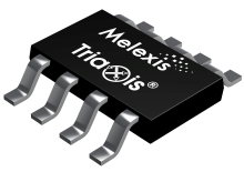
The MLX90363 is a monolithic magnetic sensor IC featuring the Tria⊗is® Hall technology. Conventional planar Hall technology is only sensitive to the flux density applied orthogonally to the IC surface. The Tria⊗is® Hall sensor is also sensitive to the flux density applied parallel to the IC surface. This is obtained through an Integrated Magneto-Concentrator (IMC) which is deposited on the CMOS die.
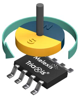
The MLX90363 is sensitive to three (B X , B Y and B Z ) components of the flux density applied to the IC. This allows the MLX90363 to sense any magnet moving in its surrounding and decode its position through an appropriate signal processing.
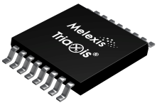
Using its Serial Interface the MLX90363 can transmit a digital output (SP – 64 bits per frame).
TSSOP-16
Absolute Contacless Position Sensor Steering Wheel Position Sensor 3D Joystick Position Sensor The MLX90363 is intended for Embedded Position Sensor applications (vs. Stand-Alone “Remote” Sensor) for which the output is directly provided to a microcontroller (Master) close to the magnetometer IC MLX90363 (Slave). The SPI protocol confirms this intent.
The MLX90363 is using full duplex SPI protocol and requires therefore the separated SPI signal lines: MOSI, MISO, /SS and SCLK.
V DD V DEC 3V3 Regulator
DSP
Triaxis ® V X V Y V
ZRAM
MUX SOIC-8 G ADC EEPROM Output Stage
14 bit SPI Angle µC
14 bit SPI XYZ ROM - Firmware MISO
MOSI
SCLK
SS V SS MLX90363 Magnetometer IC with High Speed Serial Interface Datasheet
Product Code Temperature Code Package Code Option Code Packing Form Code MLX90363 E DC ABB-000 RE MLX90363 E GO ABB-000 RE MLX90363 K DC ABB-000 RE MLX90363 K GO ABB-000 RE MLX90363 L DC ABB-000 RE MLX90363 L GO ABB-000 RE
Temperature Code: E: from -40 Deg.C to 85 Deg.C
K: from -40 Deg.C to 125 Deg.C L: from -40 Deg.C to 150 Deg.C Package Code: “DC” for SOIC-8 package
“GO” for TSSOP-16 package (dual die) Option Code: ABB-xxx: die version
xxx-000: standard Packing Form: “RE” for Reel
“TU” for Tube Ordering Example: MLX90363LGO-ABB-000-RE
Table 1 - Legend REVISION 006 – DEC 2016 Page 2 of 62 MLX90363 Magnetometer IC with High Speed Serial Interface Datasheet
Features and Benefits ................................................................................................................................... 1 Applications .................................................................................................................................................. 1 Description ................................................................................................................................................... 1 1. Ordering Information ............................................................................................................................... 2 2. Functional Diagram .................................................................................................................................. 6 3. Glossary of Terms ..................................................................................................................................... 6 4. Pinout ....................................................................................................................................................... 7 5. Pin Description ......................................................................................................................................... 8 6. Absolute Maximum Ratings ...................................................................................................................... 8 7. Electrical Specification .............................................................................................................................. 9 8. Isolation Specification ............................................................................................................................. 10 9. Timing Specification................................................................................................................................ 10
9.1. Timing Specification for 5V Application ......................................................................................... 10 9.2. Timing Specification for 3V3 Application ....................................................................................... 11 10. Accuracy Specification .......................................................................................................................... 12 11. Magnetic Specification ......................................................................................................................... 14 12. CPU & Memory Specification ............................................................................................................... 15 13. Serial Interface ..................................................................................................................................... 15
13.1. Electrical Layer and Timing Specification .................................................................................... 15 13.2. Serial Protocol .............................................................................................................................. 17 13.3. Message General Structure ......................................................................................................... 18 13.4. Regular Messages ........................................................................................................................ 20 13.4.1. Note for the regular message “X – Y – Z – diagnostic” (Marker = 2) .................................... 21 13.5. Trigger Mode 1 ............................................................................................................................. 21 13.6. Trigger Mode 2 ............................................................................................................................. 23 13.7. Trigger Mode 3 ............................................................................................................................. 24 13.8. Trigger Modes Timing Specifications ........................................................................................... 26 13.8.1. 5V Application ........................................................................................................................ 26 13.8.2. 3V3 Application ...................................................................................................................... 27 13.9. Opcode Table ............................................................................................................................... 29 13.10. Timing specifications per Opcode, and next allowed messages ............................................... 29 REVISION 006 – DEC 2016 Page 3 of 62 MLX90363 Magnetometer IC with High Speed Serial Interface Datasheet 13.11. NOP Command and NOP Answer .............................................................................................. 30 13.12. OscCounterStart and OscCounterStop Commands .................................................................. 31 13.13. Protocol Errors Handling............................................................................................................ 33 13.14. Ready, Error and NTT Messages ................................................................................................ 34 13.15. DiagnosticsDetails commands ................................................................................................... 35 13.16. MemoryRead message .............................................................................................................. 36 13.17. EEWrite Message ....................................................................................................................... 37 13.18. Reboot ........................................................................................................................................ 40 13.19. Standby ...................................................................................................................................... 40 13.20. Start-up Sequence (Serial Communication) .............................................................................. 41 13.21. Allowed sequences .................................................................................................................... 42 14. Traceability Information ....................................................................................................................... 43 15. End-User Programmable Items ............................................................................................................ 44 16. Description of End-User Programmable Items ..................................................................................... 45
16.1. User Configuration: Device Orientation ...................................................................................... 45 16.2. User Configuration: Magnetic Angle Formula ............................................................................. 45 16.3. User Configuration: 3D = 0 formula trimming parameters SMISM and ORTH_B1B2 ................ 45 16.3.1. Magnetic Angle ∠XY .............................................................................................................. 46 16.3.2. Magnetic Angle ∠XZ and ∠YZ ............................................................................................... 46 16.4. User Configuration: 3D = 1 formula trimming parameters KALPHA, KBETA, KT ........................ 47 16.5. User Configuration: Filter ............................................................................................................ 47 16.6. Virtual Gain Min and Max Parameters ........................................................................................ 47 16.7. Hysteresis Filter ............................................................................................................................ 48 16.8. EMC Filter on SCI Pins .................................................................................................................. 48 16.9. Identification & FREE bytes .......................................................................................................... 48 16.10. Lock ............................................................................................................................................ 48 17. Self Diagnostic ...................................................................................................................................... 49 18. Firmware Flowcharts ............................................................................................................................ 51
18.1. Start-up sequence ........................................................................................................................ 51 18.2. Signal Processing (GETx) .............................................................................................................. 52 18.3. Fail-safe Mode ............................................................................................................................. 52 Fail-safe mode – entry conditions ..................................................................................................... 53 18.4. Automatic Gain Control ............................................................................................................... 53 REVISION 006 – DEC 2016 Page 4 of 62 MLX90363 Magnetometer IC with High Speed Serial Interface Datasheet 19. Recommended Application Diagrams .................................................................................................. 54
19.1. MLX90363 in SOIC-8 Package and 5V Application ...................................................................... 54 19.2. MLX90363 in SOIC-8 Package and 3V3 Application .................................................................... 54 19.3. MLX90363 in TSSOP-16 Package and 5V Application ................................................................. 55 19.4. MLX90363 in TSSOP-16 Package and 3V3 Application ............................................................... 55 20. Standard information regarding manufacturability of Melexis products with different soldering
processes ............................................................................................................................................... 56 21. ESD Precautions .................................................................................................................................... 56 22. Package Information ............................................................................................................................. 57
22.1. SOIC-8 - Package Dimensions ...................................................................................................... 57 22.2. SOIC-8 - Pinout and Marking ....................................................................................................... 57 22.3. SOIC-8 - IMC Positionning ............................................................................................................ 58 22.4. TSSOP-16 - Package Dimensions ................................................................................................. 59 22.5. TSSOP-16 - Pinout and Marking ................................................................................................... 60 22.6. TSSOP-16 - IMC Positionning ....................................................................................................... 60 23. Disclaimer ............................................................................................................................................. 62 24. Contact ................................................................................................................................................. 62 REVISION 006 – DEC 2016 Page 5 of 62
MLX90363 Magnetometer IC with High Speed Serial Interface Datasheet
V DEC V DD 3V3 Regulator
DSP V X V Y V Z RAM
MUX
G ADC EEPROM Output Stage
14 bit SPI Angle µC
14 bit SPI XYZ ROM - Firmware MISO
MOSI
SCLK
SS V SS Figure 1 – Block Diagram
Gauss (G), Tesla (T) TC NC Byte Word ADC LSB MSB DNL INL RISC ASP DSP ATAN IMC CoRDiC EMC FE RE MSC FW HW Units for the magnetic flux density - 1 mT = 10 G Temperature Coefficient (in ppm/Deg.C.) Not Connected 8 bits
| Gauss (G), Tesla (T) | Units for the magnetic flux density -1 mT = 10 G |
|---|---|
| TC | Temperature Coefficient (in ppm/Deg.C.) |
| NC | Not Connected |
| Byte | 8 bits |
| Word | 16 bits (= 2 bytes) |
| ADC | Analog-to-Digital Converter |
| LSB | Least Significant Bit |
| MSB | Most Significant Bit |
| DNL | Differential Non-Linearity |
| INL | Integral Non-Linearity |
| RISC | Reduced Instruction Set Computer |
| ASP | Analog Signal Processing |
| DSP | Digital Signal Processing |
| ATAN | Trigonometric function: arctangent (or inverse tangent) |
| IMC | Integrated Magneto-Concentrator (IMC®) |
| CoRDiC | Coordinate Rotation Digital Computer (i.e. iterative rectangular-to-polar transform) |
| EMC | Electro-Magnetic Compatibility |
| FE | Falling Edge |
| RE | Rising Edge |
| MSC | Message Sequence Chart |
| FW | Firmware |
| HW | Hardware |
Table 2 – Glossary of Terms REVISION 006 – DEC 2016 Page 6 of 62 MLX90363 Magnetometer IC with High Speed Serial Interface Datasheet
| PIN | SOIC-8 | TSSOP-16 |
|---|---|---|
| 1 | V DD | V DEC1 |
| 2 | MISO | V SS1 (Ground1 ) |
| 3 | Test | V DD1 |
| 4 | SCLK | MISO1 |
| 5 | /SS | Test2 |
| 6 | MOSI | SCLK2 |
| 7 | V DEC | /SS2 |
| 8 | V SS (Ground) | MOSI2 |
| 9 | V DEC2 | |
| 10 | V SS2 (Ground2 ) | |
| 11 | V DD2 | |
| 12 | MISO2 | |
| 13 | Test1 | |
| 14 | SCLK1 | |
| 15 | /SS1 | |
| 16 | MOSI1 |
REVISION 006 – DEC 2016 Page 7 of 62 MLX90363 Magnetometer IC with High Speed Serial Interface Datasheet
Name Direction Type Function / Description V DD Supply Analog Supply (5V and 3V3 applications) MISO OUT Digital Master In Slave Out Test I/O Both Test Pin SCLK IN Digital Clock /SS IN Digital Slave Select MOSI IN Digital Master Out Slave In
5V Application V DEC I/O Analog Decoupling Pin 3V3 Application
Supply (Shorted to V DD ) V SS (Ground) GND Analog Ground
Parameter Value Supply Voltage, V DD + 18 V Reverse V DD Voltage - 0.3 V Supply Voltage, V DEC + 3.6 V Reverse V DEC Voltage - 0.3 V Positive Input Voltage + 11 V Reverse Input Voltage - 11 V Positive Output Voltage V DD + 0.3 V Reverse Output Voltage - 0.3 V Operating Ambient Temperature Range, T A - 40 Deg.C … + 150 Deg.C Storage Temperature Range, T S - 40 Deg.C … + 150 Deg.C Magnetic Flux Density ± 700 mT Exceeding the absolute maximum ratings may cause permanent damage. Exposure to absolute maximumrated conditions for extended periods may affect device reliability.
REVISION 006 – DEC 2016 Page 8 of 62 MLX90363 Magnetometer IC with High Speed Serial Interface Datasheet
| Parameter | Symbol | Test Conditions | Min | Typ | Max | Units |
|---|---|---|---|---|---|---|
| Nominal Supply Voltage | V DD5 | 5V Application | 4.5 | 5 | 5.5 | V |
| Nominal Supply Voltage | V DD33 | 3V3 Application | 3.15 | 3.3 | 3.45 | V |
| Supply Current(1) | I DD | 12.5 | 15.5 | mA | ||
| Standby Current | I STANDBY | 3.5 | 4.5 | mA | ||
| Supply Current at V DD MAX | I DDMAX | V DD = 18V | 18 | mA | ||
| POR Rising Level | POR LH | Voltage referred to V DEC | 2.6 | 2.8 | 3.1 | V |
| POR Falling Level | POR HL | Voltage referred to V DEC | 2.5 | 2.7 | 2.9 | V |
| POR Hysteresis | POR Hyst | Voltage referred to V DEC | 0.1 | V | ||
| MISO Switch Off Rising Level | MT8V LH | VDD level for disabling MISO(2) | 7.5 | 9.5 | V | |
| MISO Switch Off Falling Level | MT8V HL | VDD level for disabling MISO(2) | 6 | 7.5 | V | |
| MISO Switch Off Hysteresis | MT8V Hyst | VDD level for disabling MISO(2) | 1 | 2 | V | |
| Input High Voltage Level | V IH | 65%*V DD | - | - | V | |
| Input Low Voltage Level | V IL | - | - | 35%*V DD | V | |
| Input Hysteresis | V HYS | 20%*V DD | V | |||
| Input Capacitance | C IN | Referred to GND | 20 | pF | ||
| Output High Voltage Level | V OH | Current Drive I OH = 0.5 mA | V 0.4DD - | V | ||
| Output Low Voltage Level | V OL | Current Drive I OH = 0.5 mA | 0.4 | V | ||
| Output High Short Circuit Current | IshortH | V OUT forced to 0V | 20 | 30 | mA | |
| Isolation Resistance Between dice 4 MΩ9. Timing Specification 9.1. Timing Specification for 5V Application DC Operating Parameters at V DD = 5V (unless otherwise specified) and for TA as specified by the Temperature suffix (E, K or L). | Isolation Resistance Between dice 4 MΩ9. Timing Specification 9.1. Timing Specification for 5V Application DC Operating Parameters at V DD = 5V (unless otherwise specified) and for TA as specified by the Temperature suffix (E, K or L). | Isolation Resistance Between dice 4 MΩ9. Timing Specification 9.1. Timing Specification for 5V Application DC Operating Parameters at V DD = 5V (unless otherwise specified) and for TA as specified by the Temperature suffix (E, K or L). | Isolation Resistance Between dice 4 MΩ9. Timing Specification 9.1. Timing Specification for 5V Application DC Operating Parameters at V DD = 5V (unless otherwise specified) and for TA as specified by the Temperature suffix (E, K or L). | Isolation Resistance Between dice 4 MΩ9. Timing Specification 9.1. Timing Specification for 5V Application DC Operating Parameters at V DD = 5V (unless otherwise specified) and for TA as specified by the Temperature suffix (E, K or L). | Isolation Resistance Between dice 4 MΩ9. Timing Specification 9.1. Timing Specification for 5V Application DC Operating Parameters at V DD = 5V (unless otherwise specified) and for TA as specified by the Temperature suffix (E, K or L). | Isolation Resistance Between dice 4 MΩ9. Timing Specification 9.1. Timing Specification for 5V Application DC Operating Parameters at V DD = 5V (unless otherwise specified) and for TA as specified by the Temperature suffix (E, K or L). |
| Parameter | Symbol | Test Conditions | Min | Typ | Max | Units |
| Main Clock Frequency | Ck | 15.2 | 18.8 | MHz | ||
| Frame Rate | FR | Trigger Mode 1 (Trg. Mod. 1), Markers 0&2, SCI 2MHz | 1000 | s-1 | ||
| Frame Rate | FR | All other modes, markers and SCI Frequencies | 500 | s-1 | ||
| Watchdog time-out | Wd | See Section 17 | 15.3 | 18.8 | 20 | ms |
| Power On to First SCI message (Start-up Time) | tStartUp | See Section 13.20 | 20 | ms | ||
| SCI protocol: Slave-select rising-edge to falling-edge | tShort | 120 | µs | |||
| SCI protocol: EEWrite Time | teewrite | Trimmed oscillator | 32 | ms | ||
| Diagnostic Loop Time | tDiag | Trg.Mod.1, Markers 0&2 FR = 1000 s-1 FR = 500 s-1 FR = 200 s-1 | 10 20 40 | ms ms ms | ||
| Internal 1MHz signal | t1us | Ck = 19 MHz | 1 | µs | ||
| MISO Rise Time | CL = 30 pF, RL = 10 kΩ | 35 | 60 | ns | ||
| Magnetic Flux Density Frequency 9.2. Timing Specification DC Operating Parameters at Temperature suffix (E, K or L). | Sinewave Flux Density(3) FR = 1000 s-1 FR = 500 s-1 FR = 100 s-1 | 18 8 4 | Hz Hz Hz | |||
| Magnetic Flux Density Frequency 9.2. Timing Specification DC Operating Parameters at Temperature suffix (E, K or L). | FR = 1000 s-1 (4) 28 Hz FR = 500 s-1 (4) 14 Hz FR = 200 s-1 (4) 5.6 Hz for 3V3 Application V DD = 3.3V (unless otherwise specified) and for TA as specified by the | FR = 1000 s-1 (4) 28 Hz FR = 500 s-1 (4) 14 Hz FR = 200 s-1 (4) 5.6 Hz for 3V3 Application V DD = 3.3V (unless otherwise specified) and for TA as specified by the | FR = 1000 s-1 (4) 28 Hz FR = 500 s-1 (4) 14 Hz FR = 200 s-1 (4) 5.6 Hz for 3V3 Application V DD = 3.3V (unless otherwise specified) and for TA as specified by the | FR = 1000 s-1 (4) 28 Hz FR = 500 s-1 (4) 14 Hz FR = 200 s-1 (4) 5.6 Hz for 3V3 Application V DD = 3.3V (unless otherwise specified) and for TA as specified by the | FR = 1000 s-1 (4) 28 Hz FR = 500 s-1 (4) 14 Hz FR = 200 s-1 (4) 5.6 Hz for 3V3 Application V DD = 3.3V (unless otherwise specified) and for TA as specified by the | FR = 1000 s-1 (4) 28 Hz FR = 500 s-1 (4) 14 Hz FR = 200 s-1 (4) 5.6 Hz for 3V3 Application V DD = 3.3V (unless otherwise specified) and for TA as specified by the |
| Parameter | Symbol | Test Conditions | Min | Typ | Max | Units |
| Main Clock Frequency | Ck | 13.1 | 18.8 | MHz | ||
| Frame Rate | FR | Trigger Mode 1 (Trg. Mod. 1), Markers 0&2, SCI 2MHz | 862 | s-1 | ||
| Frame Rate | FR | All other modes, markers and SCI Frequencies | 430 | s-1 | ||
| Watchdog time-out | Wd | See Section 17 | 15.3 | 23.2 | ms | |
| Power On to First SCI message (Start-up Time) | tStartUp | See Section 13.20 | 23.2 | ms | ||
| SCI protocol: Slave-select rising-edge to falling-edge | tShort | 139 | µs | |||
| SCI protocol: EEWrite Time | teewrite | Trimmed oscillator | 37 | ms | ||
| Diagnostic Loop Time | tDiag | Trg.Mod.1, Markers 0&2 FR = 862 s-1 FR = 430 s-1 FR = 215 s-1 | 46.423.211.6 | ms ms ms | ||
| MISO Rise Time | CL = 30 pF, RL = 10 kΩ | 35 | 60 | ns | ||
| MISO Fall Time | CL = 30 pF, RL = 10 kΩ | 35 | 60 | ns | ||
| Magnetic Flux Density Frequency | FR FR FR = = = 215 430 862 s s s-1 -1 -1 (5) (5) (5) | 4.8 12 24 | Hz Hz Hz | |||
| 10. Accuracy Specification DC Operating Parameters at V DD = 5V (5V Application) or V DD = 3.3V (3V3 Application) and for TA as specified by the Temperature suffix (E, K or L). | 10. Accuracy Specification DC Operating Parameters at V DD = 5V (5V Application) or V DD = 3.3V (3V3 Application) and for TA as specified by the Temperature suffix (E, K or L). | 10. Accuracy Specification DC Operating Parameters at V DD = 5V (5V Application) or V DD = 3.3V (3V3 Application) and for TA as specified by the Temperature suffix (E, K or L). | 10. Accuracy Specification DC Operating Parameters at V DD = 5V (5V Application) or V DD = 3.3V (3V3 Application) and for TA as specified by the Temperature suffix (E, K or L). | 10. Accuracy Specification DC Operating Parameters at V DD = 5V (5V Application) or V DD = 3.3V (3V3 Application) and for TA as specified by the Temperature suffix (E, K or L). | 10. Accuracy Specification DC Operating Parameters at V DD = 5V (5V Application) or V DD = 3.3V (3V3 Application) and for TA as specified by the Temperature suffix (E, K or L). | 10. Accuracy Specification DC Operating Parameters at V DD = 5V (5V Application) or V DD = 3.3V (3V3 Application) and for TA as specified by the Temperature suffix (E, K or L). |
| Parameter | Symbol | Test Conditions | Min | Typ | Max | Units |
| ADC Resolution on the raw signals X, Y and Z | R ADC | 14 | bit | |||
| Serial Interface Resolution | R SI | On the angle value On the X,Y,Z values | 12 14 | bit bit | ||
| Offset on the Raw Signals X, Y and Z | X0, Y0, Z0 | TA = 25 Deg.C | -30 | 30 | LSB14 | |
| Mismatch on the Raw Signals X, Y and Z | SMISM XYSMISM XZSMISM YZ | TA = 25 Deg.C Between X and Y Between X and Z(6) Between Y and Z(6) | -1-30-30 | 30 30 1 | %%% | |
| Intrinsic Linearity Error(8) | Le | TA = 25 Deg.C Magnetic Angle ∠ XY Magnetic Angle ∠ XZ, ∠ YZ(9) | -1-20 | 20 1 | Deg. Deg. | |
| Supply Dependency | 5V Application V DD = 4.5 … 5.5 V | -0.1 | 0.1 | Deg. | ||
| Supply Dependency | 3V3 Application V DD = 3.20 … 3.40 V Temperature suffix E and K 20 mT 50 mT Temperature suffix L 20 mT 50 mT | -0.8-0.4-1-0.6 | 0.6 0.4 0.8 1 | Deg. Deg. Deg. Deg. | ||
| Thermal Offset Drift(10) | Temperature suffix E and K Temperature suffix L | -30-45 | 45 30 | LSB14LSB14 | ||
| Thermal Drift of Sensitivity Mismatch(11) | XY axis, XZ axis, YZ axis Temperature suffix E and K Temperature suffix L | -0.5-0.7 | 0.7 0.5 | %% | ||
| Magnetic Angle Noise(12) | Temperature suffix E and K 20mT, No Filter 50mT, No Filter 50mT, FILTER = 1 Temperature suffix L 20mT, No Filter 50mT, No Filter 50mT, FILTER = 1 | 0.20.10.070.250.120.08 | Deg. Deg. Deg. Deg. Deg. Deg. | |||
| Temperature suffix E and K 20mT, No Filter 12 LSB1450mT, No Filter 6 LSB14 Raw signals X, Y, Z Noise(12) 50mT, Temperature FILTER suffix = 1 L 4 LSB1420mT, No Filter 14 LSB1450mT, No Filter 7 LSB1450mT, FILTER = 1 4 LSB1411. Magnetic Specification DC Operating Parameters at V DD = 5V (5V Application) or V DD = 3.3V (3V3 Application) and for TA as specified by the Temperature suffix (E, K or L). | Temperature suffix E and K 20mT, No Filter 12 LSB1450mT, No Filter 6 LSB14 Raw signals X, Y, Z Noise(12) 50mT, Temperature FILTER suffix = 1 L 4 LSB1420mT, No Filter 14 LSB1450mT, No Filter 7 LSB1450mT, FILTER = 1 4 LSB1411. Magnetic Specification DC Operating Parameters at V DD = 5V (5V Application) or V DD = 3.3V (3V3 Application) and for TA as specified by the Temperature suffix (E, K or L). | Temperature suffix E and K 20mT, No Filter 12 LSB1450mT, No Filter 6 LSB14 Raw signals X, Y, Z Noise(12) 50mT, Temperature FILTER suffix = 1 L 4 LSB1420mT, No Filter 14 LSB1450mT, No Filter 7 LSB1450mT, FILTER = 1 4 LSB1411. Magnetic Specification DC Operating Parameters at V DD = 5V (5V Application) or V DD = 3.3V (3V3 Application) and for TA as specified by the Temperature suffix (E, K or L). | Temperature suffix E and K 20mT, No Filter 12 LSB1450mT, No Filter 6 LSB14 Raw signals X, Y, Z Noise(12) 50mT, Temperature FILTER suffix = 1 L 4 LSB1420mT, No Filter 14 LSB1450mT, No Filter 7 LSB1450mT, FILTER = 1 4 LSB1411. Magnetic Specification DC Operating Parameters at V DD = 5V (5V Application) or V DD = 3.3V (3V3 Application) and for TA as specified by the Temperature suffix (E, K or L). | Temperature suffix E and K 20mT, No Filter 12 LSB1450mT, No Filter 6 LSB14 Raw signals X, Y, Z Noise(12) 50mT, Temperature FILTER suffix = 1 L 4 LSB1420mT, No Filter 14 LSB1450mT, No Filter 7 LSB1450mT, FILTER = 1 4 LSB1411. Magnetic Specification DC Operating Parameters at V DD = 5V (5V Application) or V DD = 3.3V (3V3 Application) and for TA as specified by the Temperature suffix (E, K or L). | Temperature suffix E and K 20mT, No Filter 12 LSB1450mT, No Filter 6 LSB14 Raw signals X, Y, Z Noise(12) 50mT, Temperature FILTER suffix = 1 L 4 LSB1420mT, No Filter 14 LSB1450mT, No Filter 7 LSB1450mT, FILTER = 1 4 LSB1411. Magnetic Specification DC Operating Parameters at V DD = 5V (5V Application) or V DD = 3.3V (3V3 Application) and for TA as specified by the Temperature suffix (E, K or L). | Temperature suffix E and K 20mT, No Filter 12 LSB1450mT, No Filter 6 LSB14 Raw signals X, Y, Z Noise(12) 50mT, Temperature FILTER suffix = 1 L 4 LSB1420mT, No Filter 14 LSB1450mT, No Filter 7 LSB1450mT, FILTER = 1 4 LSB1411. Magnetic Specification DC Operating Parameters at V DD = 5V (5V Application) or V DD = 3.3V (3V3 Application) and for TA as specified by the Temperature suffix (E, K or L). |
| Parameter | Symbol | Test Conditions | Min | Typ | Max | Units |
| Magnetic Flux Density in X or Y | BX , BY | 20 | 50 | 70(13) | mT | |
| Magnetic Flux Density in Z | BZ | 24 | 75 | 126 | mT | |
| Magnet Temperature Coefficient | TCm | -2400 | 0 | ppm/ Deg.C | ||
| IMC Gain in X and Y(14) | GainIMCXY | 1.2 | 1.4 | 1.8 | ||
| IMC Gain in Z(14) | GainIMCZ | 1.1 | 1.3 | |||
| k factor | k | GainIMCXY / GainIMCZ | 1 | 1.2 | 1.5 | |
| ROM | 14 | KB | ||||
| RAM | 256 | B | ||||
| EEPROM | 64 | B | ||||
| CPU MIPS | Ck = 15 MHz | 3.5 | MIPS |
0.4 V 20 30 mA 25 30 mA For the dual version, the supply current is multiplied by 2 Above the MT8V threshold, no SPI communication is possible REVISION 006 – DEC 2016 Page 9 of 62 MLX90363 Magnetometer IC with High Speed Serial Interface Datasheet
Only valid for the package code GO i.e. dual die version.
Parameter Symbol Isolation Resistance Test Conditions Min Between dice 4 Typ Max Units
MΩ
DC Operating Parameters at V DD = 5V (unless otherwise specified) and for T A as specified by the Temperature suffix (E, K or L).
Parameter Main Clock Frequency Symbol Test Conditions
Ck Min Typ 15.2 Trigger Mode 1 (Trg. Mod. 1),
Frame Rate Watchdog time-out FR Markers 0&2, SCI 2MHz
All other modes, markers and SCI Frequencies Units 18.8 MHz 1000 s -1 500 s -1 20 ms Wd See Section 17 15.3 Power On to First SCI message (Start-up Time) tStartUp See Section 13.20 20 ms SCI protocol: Slave-select rising-edge to falling-edge tShort 120 µs SCI protocol: EEWrite Time teewrite 32 ms Trimmed oscillator 18.8 Max Diagnostic Loop Time Internal 1MHz signal
Page 10 of 62
Datasheet Parameter Symbol Test Conditions Min Typ Max Units
Sinewave Flux Density (3)
DC Operating Parameters at V DD = 3.3V (unless otherwise specified) and for T A as specified by the Temperature suffix (E, K or L).
Parameter Main Clock Frequency Symbol Test Conditions
Ck Min Typ 13.1 Trigger Mode 1 (Trg. Mod. 1),
Frame Rate Watchdog time-out FR Markers 0&2, SCI 2MHz
All other modes, markers and SCI Frequencies Max Units 18.8 MHz 862 s -1 430 s -1 23.2 ms Wd See Section 17 15.3 Power On to First SCI message (Start-up Time) tStartUp See Section 13.20 23.2 ms SCI protocol: Slave-select rising-edge to falling-edge tShort 139 µs SCI protocol: EEWrite Time teewrite 37 ms Trimmed oscillator Diagnostic Loop Time Internal 1MHz signal tDiag t1us
3 Sensitivity monitors enabled (See section 17). Beyond that frequency, the Sensitivity monitor must be disabled. Contact Melexis for more details. 4 Limitation linked to the Automatic Gain Control. Beyond that frequency, there is a reduced immunity to norm change (e.g. through vibration). See also Section 18.4 REVISION 006 – DEC 2016 Page 11 of 62
Datasheet Parameter Symbol Test Conditions Min Typ Max Units MISO Rise Time C L = 30 pF, R L = 10 kΩ 35 60 ns MISO Fall Time C L = 30 pF, R L = 10 kΩ 35 60 ns
Magnetic Flux Density Frequency
DC Operating Parameters at V DD = 5V (5V Application) or V DD = 3.3V (3V3 Application) and for T A as specified by the Temperature suffix (E, K or L).
Parameter Symbol ADC Resolution on the raw signals X, Y and Z R ADC Serial Interface Resolution R SI Offset on the Raw Signals X, Y and Z X0, Y0, Z0 Test Conditions Min Typ Max Units 14 bit On the angle value 14 bit On the X,Y,Z values 12 bit
Mismatch on the Raw Signals X, Y and Z SMISM XY SMISM XZ SMISM YZ Between X and Z (6) -30 30 % Between Y and Z (6) -30 30 %
Magnetic Angle Phase Error ORTH XY ORTH XZ
ORTH YZ Between X and Y -0.3 0.3 Deg. Between X and Z (7) -10 10 Deg. Between Y and Z (7) -10 10 Deg.
5 Limitation linked to the Automatic Gain Control. Beyond that frequency, there is a reduced immunity to norm change (e.g. through vibration). See also Section 18.4 6 The Mismatch between X or Y and Z can be reduced through the calibration of the SMISM (or k) factor in the end application. See section 16.3.2 for more information 7 The Magnetic Angle Phase error X or Y and Z can be reduced through the calibration of the ORTH_B1B2 factor in the end application. See section 16.3.2 for more information REVISION 006 – DEC 2016 Page 12 of 62
Datasheet Parameter Symbol Test Conditions Min Typ Max Units -1 1 Deg. -20 20 Deg.
-0.1 0.1 Deg.
20 mT -0.8 0.8 Deg. 50 mT -0.4 0.4 Deg.
20 mT -1 1 Deg. 50 mT -0.6 0.6 Deg. Temperature suffix E and K -30 30 LSB 14 Temperature suffix L -45 45 LSB 14
XY axis, XZ axis, YZ axis Temperature suffix E and K -0.5 0.5 % Temperature suffix L -0.7 0.7 % XY axis, XZ axis, YZ axis -0.1 0.1 Deg.
Intrinsic Linearity Error (8) Le Magnetic Angle ∠ XY
Magnetic Angle ∠ XZ, ∠ YZ (9) 5V Application
3V3 Application
Supply Dependency Temperature suffix E and K Temperature suffix L Thermal Offset Drift (10)
Thermal Drift of Sensitivity Mismatch (11)
Thermal Drift of Magnetic Angle Phase Error 8 The Intrinsic Linearity Error is a consolidation of the IC errors (offset, sensitivity mismatch, phase error) taking into account an ideal rotating field. Once associated to a practical magnetic construction and the associated mechanical and magnetic tolerances, the output linearity error increases. 9 The Intrisic Linearity Error for Magnetic Angle ∠ XZ, ∠ YZ can be reduced through the programming of the SMISM (or k) factor and ORTH_B1B2. By applying the correct compensation, a non linearity error of +/-1 Deg. can be reached. See section 16.3.2 for more information 10 For instance, Thermal Offset Drift equal ± 30 LSB
14 yields to max. ± 0.32 Deg. error. This is only valid if the Virtual Gain is not fixed (See Section 18.4). See Front End Application Note for more details 11 For instance, Thermal Drift of Sensitivity Mismatch equal ± 0.4 % yields to max. ± 0.1 Deg. error. See Front End Application Note for more details REVISION 006 – DEC 2016 Page 13 of 62
Datasheet Parameter Symbol Test Conditions Min Typ Max Units 20mT, No Filter 0.2 Deg. 50mT, No Filter 0.1 Deg.
20mT, No Filter 0.25 Deg. 50mT, No Filter 0.12 Deg.
20mT, No Filter 12 LSB 14 50mT, No Filter 6 LSB 14 50mT, FILTER = 1 4 LSB 14 20mT, No Filter 14 LSB 14 50mT, No Filter 7 LSB 14 50mT, FILTER = 1 4 LSB 14 Temperature suffix E and K Magnetic Angle Noise (12) Temperature suffix L Temperature suffix E and K Raw signals X, Y, Z Noise (12) Temperature suffix L
DC Operating Parameters at V DD = 5V (5V Application) or V DD = 3.3V (3V3 Application) and for T A as specified by the Temperature suffix (E, K or L).
Parameter Symbol Magnetic Flux Density in X or Y Min Typ Max Units B X , B Y 20 50 70 (13) mT Magnetic Flux Density in Z B Z 24 75 126 mT
Magnet Temperature Coefficient TCm -2400
IMC Gain in X and Y (14) GainIMC XY 1.2 IMC Gain in Z (14) GainIMC Z 1.1 k factor k Test Conditions GainIMC XY / GainIMC Z 1 ppm/ 0 1.4 Deg.C 1.8 1.3 1.2 1.5 12 Noise is defined by ± 3 σ for 1000 successive acquisitions. The application diagram used is described in the recommended wiring (Section 20). For detailed information, refer to section Filter in application mode (Section 16.5). 13 Above 70 mT, the IMC starts saturating yielding to an increase of the linearity error. 14 This is the magnetic gain linked to the Integrated Magneto Concentrator structure. This is the overall variation. Within one lot, the part to part variation is typically ± 10% versus the average value of the IMC gain of that lot.
REVISION 006 – DEC 2016 Page 14 of 62
Datasheet
The digital signal processing is based on a 16 bit RISC µController featuring
ROM & RAM EEPROM with hamming codes (ECC) Watchdog C Compiler
Parameter Symbol Test Conditions Min Typ Max Units ROM 14 KB RAM 256 B EEPROM 64 B 3.5 MIPS CPU MIPS Ck = 15 MHz
The MLX90363 serial interface allows a Master device to operate the position sensor. The MLX90363 interface allows Multi-Slave applications and synchronous start of the data acquisition among the Slaves. The interface offers 2 Mbps data transfer bit rate and is full duplex. The interface accepts messages of 64 bits wide only, making the interfacing robust.
In this document, the words message, frame and packet refer to the same concept.
Message transmissions start necessarily at a falling edge on /SS and end necessarily at a rising edge on the /SS signal. This defines a message. The serial interface counts the number of transmitted bits and declares the incoming message invalid when the bit count differs from 64. The Master must therefore ensure the flow described below:
REVISION 006 – DEC 2016 Page 15 of 62
Datasheet The MISO and MOSI signals change on SCLK rising edge and are captured on SCLK falling edge. The mostsignificant-bit of the transmitted byte or word comes first (15) .
| MOSI Pin MISO Pin The interface is sensitive, on /SS, while SCLK is kept /SS Pin (IC PIN) | tMOSI | |||||||
|---|---|---|---|---|---|---|---|---|
| MOSI Pin MISO Pin The interface is sensitive, on /SS, while SCLK is kept /SS Pin (IC PIN) | tMOSI | tMOSI | tMOSI | tMOSI | tMOSI | tMOSI | ||
| MOSI Pin MISO Pin The interface is sensitive, on /SS, while SCLK is kept /SS Pin (IC PIN) | t2 tMISO t4 Figure 2 – Serial Interface Timing Diagram in Trigger mode 2 (see section 13.6), to Sync pulses. A Sync pulse is negative pulse quiet. tSyncPulse Figure 3 – Sync Pulse Timing Diagram | t2 tMISO t4 Figure 2 – Serial Interface Timing Diagram in Trigger mode 2 (see section 13.6), to Sync pulses. A Sync pulse is negative pulse quiet. tSyncPulse Figure 3 – Sync Pulse Timing Diagram | t2 tMISO t4 Figure 2 – Serial Interface Timing Diagram in Trigger mode 2 (see section 13.6), to Sync pulses. A Sync pulse is negative pulse quiet. tSyncPulse Figure 3 – Sync Pulse Timing Diagram | t2 tMISO t4 Figure 2 – Serial Interface Timing Diagram in Trigger mode 2 (see section 13.6), to Sync pulses. A Sync pulse is negative pulse quiet. tSyncPulse Figure 3 – Sync Pulse Timing Diagram | t2 tMISO t4 Figure 2 – Serial Interface Timing Diagram in Trigger mode 2 (see section 13.6), to Sync pulses. A Sync pulse is negative pulse quiet. tSyncPulse Figure 3 – Sync Pulse Timing Diagram | t2 tMISO t4 Figure 2 – Serial Interface Timing Diagram in Trigger mode 2 (see section 13.6), to Sync pulses. A Sync pulse is negative pulse quiet. tSyncPulse Figure 3 – Sync Pulse Timing Diagram | t2 tMISO t4 Figure 2 – Serial Interface Timing Diagram in Trigger mode 2 (see section 13.6), to Sync pulses. A Sync pulse is negative pulse quiet. tSyncPulse Figure 3 – Sync Pulse Timing Diagram | t2 tMISO t4 Figure 2 – Serial Interface Timing Diagram in Trigger mode 2 (see section 13.6), to Sync pulses. A Sync pulse is negative pulse quiet. tSyncPulse Figure 3 – Sync Pulse Timing Diagram |
| Parameter | Parameter | Symbol | Symbol | Test Conditions | Min | Typ | Max | Units |
| Clock Period | Clock Period | tSCLK | tSCLK | EE_PINFILTER = 1 EE_PINFILTER = 2 EE_PINFILTER = 3 | 4509001800 | 50010002000 | ns ns ns | |
| Clock Low Level | Clock Low Level | tSCLK_HI | tSCLK_HI | EE_PINFILTER = 1 EE_PINFILTER = 2 EE_PINFILTER = 3 | 225450900 | ns ns ns | ||
| Clock High Level | Clock High Level | tSCLK_LO | tSCLK_LO | EE_PINFILTER = 1 EE_PINFILTER = 2 EE_PINFILTER = 3 | 225450900 | ns ns ns | ||
| Clock to Data Delay | Clock to Data Delay | tMISO | tMISO | EE_PINFILTER = 1, CL = 30pF EE_PINFILTER = 2, CL = 30pF EE_PINFILTER = 3, CL = 30pF | 210300510 | ns ns ns | ||
30 ns 15 For instance, for Master compatible w/ the Motorola SPI protocol, the configuration bits must be CPHA=1, CPOL=0, LSBFE=0.
REVISION 006 – DEC 2016 Page 16 of 62
Datasheet Parameter /SS FE to SCLK RE /SS FE to MISO Low Impedance SCLK FE to /SS RE /SS RE to MISO High Impedance Sync Pulse Duration Symbol t1 t2 Test Conditions Min
tSyncPulse Max Units
t3 t4 Typ 225 ns
Table 3 – Serial Interface Timing Specifications
Melexis recommends using the Multi-Slave application diagram as shown on the right.
The SCLK, MISO and MOSI wires interconnect the Slaves with the Master. A Slave is selected by its dedicated /SS input. A Slave MISO output is in high-impedance state when the Slave is not selected.
Slave 1 Master
SCLK MOSI MISO SS1 SS2 SS3 SCLK MOSI MISO SS
Slave 2 SCLK MOSI MISO SS Slave 3 Slaves can be triggered synchronously by sending Sync pulses on the different /SS. The pulses must not overlap to avoid electrical short-circuits on the MISO bus.
SCLK MOSI MISO SS
The serial protocol of MLX90363 allows the SPI Master device to request the following information:
Position (magnetic angle Alpha) Raw field components (X,Y and Z) Self-Diagnostic data
It allows customizing the calibration of the sensor, when needed, at the end-of-line, through EEPROM programming.
The serial protocol offers a transfer rate of 1000 messages/sec. A regular message holds position and diagnostic information. The data acquisition start and processing is fully under the control of the SPI Master. The user configuration bits, stored in EEPROM, are programmable with this protocol.
REVISION 006 – DEC 2016 Page 17 of 62
Datasheet Data integrity is guaranteed in both directions by an 8 bit CRC covering the content of the incoming and outgoing messages.
A message has a unique Opcode. The general structure of a message consists of 8 bytes (byte #0, transmitted first, to byte #7 transmitted last).
Byte #7 (the last byte transmitted) holds an 8 bit CRC. The byte #6 holds a Marker plus either an Opcode or a rolling counter (6 bit Roll Counter).
6 5 4 3 3 1 0
(3)
6 5 4 3 2 1 2 5 7 2 0
(1) (5) 4 CRC 6 Marker Opcode or Roll Counter
Table 4 – General Structure of a message and bit naming convention
(1) This bit is named Byte0[0] (2) This bit is named Byte0[7]
(3) This bit is named Byte1[0] (4) This bit is named Byte1[7]
(5) This bit is named Byte2[0]
A blank cell refers necessarily to a bit 0.
In a byte, the most-significant-bit is transmitted first (for instance, Byte0[7] is transmitted first, Byte0[0] transmitted last).
Parameter CRC[7:0] is Byte7[7:0], Parameter Marker[1:0] is Byte6[7:6],
Parameter Opcode[5:0] (or Roll Counter[5:0]) is Byte6[5:0]
CRCs are encoded and decoded according the following algorithm (language-C):
crc = 0xFF; crc = cba_256_TAB[ Byte0 ^ crc ]; crc = cba_256_TAB[ Byte1 ^ crc ]; crc = cba_256_TAB[ Byte2 ^ crc ]; crc = cba_256_TAB[ Byte3 ^ crc ]; crc = cba_256_TAB[ Byte4 ^ crc ]; crc = cba_256_TAB[ Byte5 ^ crc ]; crc = cba_256_TAB[ Byte6 ^ crc ]; crc = ~crc;
The Table 5 corresponds to the CRC-8 polynomial “0xC2”.
REVISION 006 – DEC 2016 Page 18 of 62
| cba_256_TAB | 0 | 1 | 2 | 3 | 4 | 5 | 6 | 7 |
|---|---|---|---|---|---|---|---|---|
| 0 | 0x00 | 0x2f | 0x5e | 0x71 | 0xbc | 0x93 | 0xe2 | 0xcd |
| 1 | 0x57 | 0x78 | 0x09 | 0x26 | 0xeb | 0xc4 | 0xb5 | 0x9a |
| 2 | 0xae | 0x81 | 0xf0 | 0xdf | 0x12 | 0x3d | 0x4c | 0x63 |
| 3 | 0xf9 | 0xd6 | 0xa7 | 0x88 | 0x45 | 0x6a | 0x1b | 0x34 |
| 4 | 0x73 | 0x5c | 0x2d | 0x02 | 0xcf | 0xe0 | 0x91 | 0xbe |
| 5 | 0x24 | 0x0b | 0x7a | 0x55 | 0x98 | 0xb7 | 0xc6 | 0xe9 |
| 6 | 0xdd | 0xf2 | 0x83 | 0xac | 0x61 | 0x4e | 0x3f | 0x10 |
| 7 | 0x8a | 0xa5 | 0xd4 | 0xfb | 0x36 | 0x19 | 0x68 | 0x47 |
| 8 | 0xe6 | 0xc9 | 0xb8 | 0x97 | 0x5a | 0x75 | 0x04 | 0x2b |
| 9 | 0xb1 | 0x9e | 0xef | 0xc0 | 0x0d | 0x22 | 0x53 | 0x7c |
| 10 | 0x48 | 0x67 | 0x16 | 0x39 | 0xf4 | 0xdb | 0xaa | 0x85 |
| 11 | 0x1f | 0x30 | 0x41 | 0x6e | 0xa3 | 0x8c | 0xfd | 0xd2 |
| 12 | 0x95 | 0xba | 0xcb | 0xe4 | 0x29 | 0x06 | 0x77 | 0x58 |
| 13 | 0xc2 | 0xed | 0x9c | 0xb3 | 0x7e | 0x51 | 0x20 | 0x0f |
| 14 | 0x3b | 0x14 | 0x65 | 0x4a | 0x87 | 0xa8 | 0xd9 | 0xf6 |
| 15 | 0x6c | 0x43 | 0x32 | 0x1d | 0xd0 | 0xff | 0x8e | 0xa1 |
| 16 | 0xe3 | 0xcc | 0xbd | 0x92 | 0x5f | 0x70 | 0x01 | 0x2e |
| 17 | 0xb4 | 0x9b | 0xea | 0xc5 | 0x08 | 0x27 | 0x56 | 0x79 |
| 18 | 0x4d | 0x62 | 0x13 | 0x3c | 0xf1 | 0xde | 0xaf | 0x80 |
| 19 | 0x1a | 0x35 | 0x44 | 0x6b | 0xa6 | 0x89 | 0xf8 | 0xd7 |
| 20 | 0x90 | 0xbf | 0xce | 0xe1 | 0x2c | 0x03 | 0x72 | 0x5d |
| 21 | 0xc7 | 0xe8 | 0x99 | 0xb6 | 0x7b | 0x54 | 0x25 | 0x0a |
| 22 | 0x3e | 0x11 | 0x60 | 0x4f | 0x82 | 0xad | 0xdc | 0xf3 |
| 23 | 0x69 | 0x46 | 0x37 | 0x18 | 0xd5 | 0xfa | 0x8b | 0xa4 |
| 24 | 0x05 | 0x2a | 0x5b | 0x74 | 0xb9 | 0x96 | 0xe7 | 0xc8 |
| 25 | 0x52 | 0x7d | 0x0c | 0x23 | 0xee | 0xc1 | 0xb0 | 0x9f |
| 26 | 0xab | 0x84 | 0xf5 | 0xda | 0x17 | 0x38 | 0x49 | 0x66 |
| 27 | 0xfc | 0xd3 | 0xa2 | 0x8d | 0x40 | 0x6f | 0x1e | 0x31 |
| 28 | 0x76 | 0x59 | 0x28 | 0x07 | 0xca | 0xe5 | 0x94 | 0xbb |
| 29 | 0x21 | 0x0e | 0x7f | 0x50 | 0x9d | 0xb2 | 0xc3 | 0xec |
| 30 | 0xd8 | 0xf7 | 0x86 | 0xa9 | 0x64 | 0x4b | 0x3a | 0x15 |
| 31 | 0x8f | 0xa0 | 0xd1 | 0xfe | 0x33 | 0x1c | 0x6d | 0x42 |
Table 5 – cba_256_TAB Look-up table Polynomial “C2” REVISION 006 – DEC 2016 Page 19 of 62
Datasheet # 1 7 6 5 4 3
0xFF 2 1 0 #
0 7 6 5 4 3
0xC1 3 0xFF 2 0x16 5 0xFF 4 0xD4 7 0x23 6 0x86 2 1 0 Table 6 – Example of valid CRC
The MLX90363 offers three types of regular messages:
“α” – diagnostic “α – β” – diagnostic X – Y – Z – diagnostic
ALPHA [13:8] 0 #
0 7 6 5 4 3 2
ALPHA [7:0] 3 0 2 0 5 0 4 VG[7:0] 7 CRC 6 0 0 1 0 ROLL
Table 7 – “α” message # 1 7 E1 6 E0 5 3 4 3 2 1
ALPHA [13:8] 0 #
0 BETA [13:8] 2 5 0 4 7 CRC 6 7 6 5 4 3 2
ALPHA [7:0] 1 0 BETA [7:0] VG[7:0] 0 1 ROLL
Table 8 – “α – β” message # 1 7 E1 6 E0 5 4 3 2 1
X COMPONENT [13:8] 0 #
0 7 6 5 4 3 2
X COMPONENT [7:0] 3 Y COMPONENT [13:8] 2 Y COMPONENT [7:0] 5 Z COMPONENT [13:8] 4 Z COMPONENT [7:0] 7 CRC 6 1 0 1 0 ROLL Table 9 – “X – Y – Z” message
The bits Byte6[7] and Byte6[6] are markers. They allow the Master to recognize the type of regular message (00b, 01b, 10b). The marker is present in all messages (incoming and outgoing). The marker of any message which is not a regular message is equal to 11b.
The bits E1 and E0 report the status of the diagnostics (4 possibilities) as described in the Table 10 – See section 17 for more details.
REVISION 006 – DEC 2016 Page 20 of 62
| E1 | E0 | Description |
|---|---|---|
| 0 | 0 | First Diagnostics Sequence Not Yet Finished |
| 0 | 1 | Diagnostic Fail |
| 1 | 0 | Diagnostic Pass (Previous cycle) |
| 1 | 1 | Diagnostic Pass – New Cycle Completed |
Table 10 - Diagnostics Status Bits
In the case of Marker = 2d, the X, Y, Z components are given after offset compensation and filtering (see signal processing in section 18.2). These components are gain dependent (see also section 18.4).
Although being 12 bit resolution signals, the X, Y, Z components are coded on 14 bits. For proper decoding, the values must be shifted twice to the left in order to get a 16 bit signed value (2’s complementary).
The sensitivity in the X and Y direction is always higher than the Z direction by the IMC Gain factor (see parameter k factor in section 11). Melexis therefore recommends multiplying the Z component by the k factor inside the Master in order to use the MLX90363 as a 3D magnetometer.
The Master sends a GET1 command to initiate the magnetic field acquisition and post-processing. It waits tSSREFE, issues the next GET1 and receives at the same time the regular message resulting from the previous GET.
The field sensing, acquisition and post-processing is starting on /SS rising edge events.
Although GET1 commands are preferably followed by another GET1 command or a NOP command, any other commands are accepted by the Slave.
FW SPI HW background Get
tSSREFE SPI ASP DSP SPI ASP DSP SPI ASP DSP SPI Get Get NOP
XFigure 4 – Trigger Mode 1 REVISION 006 – DEC 2016 Page 21 of 62
Datasheet Message Sequence Chart Single Slave - Mode 1
Slave Master
GET1 ( à ) NTT ( ß )
Loop
GET1 ( à ) Regular Packet ( ß )
NOP ( à ) Regular Packet ( ß )
Figure 5 – Trigger Mode 1 Message Sequence Chart # 1 7 3 5 7 6 5 4 3 2 1 0
RST Time – Out CRC # 0 2 4 6 7 6 5 4 3 2 1 0 0 1 1 Value Marker 0 1 0 Table 11 – GET1 MOSI Message (Opcode = 19d)
Note: The NOP message is described at section 13.11.
The parameter Marker defines the regular data packet type expected by the Master:
Marker = 0 refers to frame type “ALPHA + Diagnostic”. Marker = 1 refers to frame type “ALPHA + BETA + Diagnostic”. Marker = 2 refers to frame type “Components X + Y + Z +Diagnostic”.
The parameter RST (Byte1[0]) when set, resets the rolling counter attached to the regular data packets.
The parameter TimeOutValue tells the maximum life time of the Regular Data Message.
The time step is t1us (See table in Section 9), the maximum time-out is 65535 * t1us. The time-out timer starts when the message is ready, and stops on the /SS rising edge of the next message.
On time-out occurrence, there are two possible scenarios:
Scenario 1: /SS is high, there is no message exchange. In this case, a NTT message replaces the
regular message in the SCI buffer. Scenario 2: /SS is low, the regular packet is being sent out. In this case, the timeout violation is
reported on the next message, this later being an NTT message.
The master must handle the NTT errors as described in Table 30 – Protocol Errors Handling (Master standpoint).
REVISION 006 – DEC 2016 Page 22 of 62
Datasheet
The Trigger Mode 1 works without Sync pulses, as the GET1 command plays the role of a sync pulse. When a delay between the regular message readback and the start of acquisition is needed, or when two or more Slaves should be triggered synchronously, the use of a sync pulse is required, and this is the meaning of the Trigger Mode 2.
Principle: The Master first enables the trigger mode 2 by issuing a GET2 command.
The Master then sends a Sync Pulse, at the appropriate time, to initiate the magnetic field acquisition and post-processing.
Finally the Master reads the response message with a NOP or a GET2. The GET2 command re-initiates a sync pulse triggered acquisition, whereas the NOP command would just allow the Master to receive the latest packet.
| FW1 background SP I ASP DSP SPI SP I | ASP DSP SPI | SP I |
|---|---|---|
| SPI HW1 Get2 Get2 | Get2 | |
| FW2 background SP I ASP DSP SPI SP I | ASP DSP SPI | SP I |
| SPI HW2 Get2 Sync Puls Get2 | Sync Puls | Get2 |
| Get2 for Slave 1 and Get2 for Slave 2 do not overlap |
tSyncFE Figure 6 – Trigger Mode 2 – Single Slave Approach
A timing constraint between GET2 and the Sync pulse (tRESync) should be met.
When this timing is smaller than the constraint, the sync pulse might not be taken in account, causing the next GET2 to return a NTT packet.
GET1 and GET2/Sync pulse can be interlaced.
Multi-Slave approach: The way of working described below fits the Multi-Slave applications where synchronous acquisitions are important. GET2 commands are sent one after the other to the Slaves. Then the Sync pulses are sent almost synchronously (very shortly one after the other).
FW1 SPI HW1 FW2 SP background
| FW background SP I SP I ASP DSP SPI | SP I | SP I ASP DSP SPI | SP I |
|---|---|---|---|
| SPI HW Get2 Sync Puls | Get2 | Sync Puls | Get2 |
| tRESync | tSyncFE |
Get2 for Slave 1 and Get2 for Slave 2 do not overlap
Figure 7 – Trigger Mode 2 – Multi-Slave approach, example for two Slaves REVISION 006 – DEC 2016 Page 23 of 62
Datasheet Message Sequence Chart Dual Slave - Mode 2 (Sync pulses)
Slave2 Slave1 Master
GET2 ( à ) NTT ( ß )
GET2 ( à ) NTT ( ß ) Sync Pulse Loop GET2 ( à )
Regular Packet ( ß )
GET2 ( à ) Regular Packet ( ß ) Sync Pulse NOP ( à ) Regular Packet ( ß )
NOP ( à ) Regular Packet ( ß )
Figure 8 – Trigger Mode 2 Message Sequence Chart # 1 7 6 5 3 5 7 4 3 2 Time – Out CRC 1 0
RST # 0 2 4 6 7 6 5 4 3 2 1 0 1 0 0 Value Marker 0 1 0 Table 12 – GET2 MOSI Message (Opcode = 20d)
Parameter definition: See GET1 (Section 13.5).
Principle: The acquisition sequences are triggered by a GET message, but unlike the Mode 1, the resulting data (position …) is buffered. The MISO messages contain the buffered data of the previous GET message, and not the newly computed values corresponding to the current GET MOSI request. The buffering releases constraints on the SCI clock frequency (SCLK). The Mode 3 offers frame rates as high as Mode 1, if not higher, with slower SCLK frequencies. When the clock frequency is limited (400 kbps or less), and when it matters to reach a certain frame rate, Mode 3 is preferred over Mode 1. In any other cases, for instance when the shortest response time represents the main design criteria, Mode 1 is preferred.
REVISION 006 – DEC 2016 Page 24 of 62
Datasheet FW background SPI HW ASP SPI SP DSP SPI ASP ASP I DSP Get3 Get3
DSP DSP ASP SPI Get3 tSSREFE_ SPI DSP NOP Roll=1 X Roll=2 Figure 9 – Trigger Mode 3
GET3 sequences must end with a NOP.
Message Sequence Chart Single Slave - Mode 3
Master Slave
GET3 ( à ) X ( ß ) GET3 ( à ) Get3Ready ( ß )
Loop GET3 ( à )
Regular Packet ( ß )
NOP ( à ) Regular Packet ( ß )
Figure 10 – Trigger Mode 3 Message Sequence Chart # 1 7 6 5 4 3 2 1 0
RST Time – Out 3 5 7 # 0 2 4 6 CRC 7 6 5 4 3 2 1 0 1 0 1 Value Marker 0 1 0 Table 13 – GET3 MOSI Message (Opcode = 21d)
Parameter definition: See GET1 (Section 13.5)
0 2 4 6 7 6 5 4 3 2 1 0 1 1 1 0 1 1 0 1 Table 14 – Get3Ready MISO Message (Opcode = 45d)
REVISION 006 – DEC 2016 Page 25 of 62
MLX90363 Magnetometer IC with High Speed Serial Interface Datasheet
/SS Pin GET1 GET1 tREFE_mod1 SCI Internal state High: NTT Low: Ready tReady_mod1 Figure 11 – Trigger Mode 1 timing diagram /SS Pin SyncPulse GET2 GET2
tRESync SCI Internal state High: NTT Low: Ready tSyncFE tReady_mod2
Figure 12 – Trigger Mode 2 timing diagram /SS Pin GET3 SCI Internal state High: NTT Low: Ready GET3 tREFE_mod3 tReady_FEmod3 tRERE_mod3 tReady_REmod3 High: DSP Ongoing
Figure 13 – Trigger Mode 3 timing diagram
| Items | Definition | Marker | Min | Typ | Max | Unit |
|---|---|---|---|---|---|---|
| tREFE_mod1 | Get1 SS Rising Edge to next Get1 SS Falling Edge | 0 | 920 | μs | ||
| tREFE_mod1 | Get1 SS Rising Edge to next Get1 SS Falling Edge | 1 | 1050 | μs | ||
| tREFE_mod1 | Get1 SS Rising Edge to next Get1 SS Falling Edge | 2 | 920 | μs | ||
| tReady_mod1 | Get1 SSRE to SO Answer ReadyToTransmit | 0 | 920 | μs | ||
| tReady_mod1 | Get1 SSRE to SO Answer ReadyToTransmit | 1 | 1050 | μs | ||
| tReady_mod1 | Get1 SSRE to SO Answer ReadyToTransmit | 2 | 920 | μs |
Table 15 – Trigger Mode 1 Timing Specification (V DD =5V)
REVISION 006 – DEC 2016 Page 26 of 62 MLX90363 Magnetometer IC with High Speed Serial Interface Datasheet Items tSyncFE tReady_mod2 tRESync Definition Sync Pulse (RE) to Get2 Falling Edge Sync Pulse (RE) to SO Answer ReadyToTransmit Marker Min Typ Max Unit
| Items | Definition | Marker | Min | Typ | Max | Unit | |||
|---|---|---|---|---|---|---|---|---|---|
| tSyncFE | Sync Pulse (RE) to Get2 Falling Edge | Sync Pulse (RE) to Get2 Falling Edge | 0 | 0 | 874 | 874 | μs | ||
| tSyncFE | Sync Pulse (RE) to Get2 Falling Edge | Sync Pulse (RE) to Get2 Falling Edge | 1 | 1 | 1004 | 1004 | μs | ||
| tSyncFE | Sync Pulse (RE) to Get2 Falling Edge | Sync Pulse (RE) to Get2 Falling Edge | 2 | 2 | 874 | 874 | μs | ||
| tReady_mod2 | Sync Pulse (RE) to SO Answer ReadyToTransmit | Sync Pulse (RE) to SO Answer ReadyToTransmit | 0 | 0 | 874 | μs | |||
| tReady_mod2 | Sync Pulse (RE) to SO Answer ReadyToTransmit | Sync Pulse (RE) to SO Answer ReadyToTransmit | 1 | 1 | 1004 | μs | |||
| tReady_mod2 | Sync Pulse (RE) to SO Answer ReadyToTransmit | Sync Pulse (RE) to SO Answer ReadyToTransmit | 2 | 2 | 874 | μs | |||
| tRESync Get2 SS Rising Edge to Sync Pulse (RE) 80 μs Table 16 – Trigger Mode 2 Timing Specification (V DD =5V) | tRESync Get2 SS Rising Edge to Sync Pulse (RE) 80 μs Table 16 – Trigger Mode 2 Timing Specification (V DD =5V) | tRESync Get2 SS Rising Edge to Sync Pulse (RE) 80 μs Table 16 – Trigger Mode 2 Timing Specification (V DD =5V) | tRESync Get2 SS Rising Edge to Sync Pulse (RE) 80 μs Table 16 – Trigger Mode 2 Timing Specification (V DD =5V) | tRESync Get2 SS Rising Edge to Sync Pulse (RE) 80 μs Table 16 – Trigger Mode 2 Timing Specification (V DD =5V) | tRESync Get2 SS Rising Edge to Sync Pulse (RE) 80 μs Table 16 – Trigger Mode 2 Timing Specification (V DD =5V) | tRESync Get2 SS Rising Edge to Sync Pulse (RE) 80 μs Table 16 – Trigger Mode 2 Timing Specification (V DD =5V) | tRESync Get2 SS Rising Edge to Sync Pulse (RE) 80 μs Table 16 – Trigger Mode 2 Timing Specification (V DD =5V) | tRESync Get2 SS Rising Edge to Sync Pulse (RE) 80 μs Table 16 – Trigger Mode 2 Timing Specification (V DD =5V) | tRESync Get2 SS Rising Edge to Sync Pulse (RE) 80 μs Table 16 – Trigger Mode 2 Timing Specification (V DD =5V) |
| Items | Items | Definition | Definition | Marker | Marker | Min | Typ | Max | Unit |
| tRERE_mod3 | tRERE_mod3 | Get3 SS RE to RE | Get3 SS RE to RE | 0 | 0 | 950 | μs | ||
| tRERE_mod3 | tRERE_mod3 | Get3 SS RE to RE | Get3 SS RE to RE | 1 | 1 | 1080 | μs | ||
| tRERE_mod3 | tRERE_mod3 | Get3 SS RE to RE | Get3 SS RE to RE | 2 | 2 | 950 | μs | ||
| tReadyRE_mod3 | tReadyRE_mod3 | Get3 SS RE to DSP Completion | Get3 SS RE to DSP Completion | 0 | 0 | 950 | μs | ||
| tReadyRE_mod3 | tReadyRE_mod3 | Get3 SS RE to DSP Completion | Get3 SS RE to DSP Completion | 1 | 1 | 1080 | μs | ||
| tReadyRE_mod3 | tReadyRE_mod3 | Get3 SS RE to DSP Completion | Get3 SS RE to DSP Completion | 2 | 2 | 950 | μs | ||
| tREFE_mod3 | tREFE_mod3 | Get3 SS Rising to Falling | Get3 SS Rising to Falling | 90 | μs | ||||
| tReadyFE_mod3 | tReadyFE_mod3 | Get3 SS RE to SO Answer ReadyToTransmit | Get3 SS RE to SO Answer ReadyToTransmit | 90 | μs | ||||
| Table 17 – Trigger Mode 3 Timing Specification (V DD =5V)13.8.2. 3V3 Application | Table 17 – Trigger Mode 3 Timing Specification (V DD =5V)13.8.2. 3V3 Application | Table 17 – Trigger Mode 3 Timing Specification (V DD =5V)13.8.2. 3V3 Application | Table 17 – Trigger Mode 3 Timing Specification (V DD =5V)13.8.2. 3V3 Application | Table 17 – Trigger Mode 3 Timing Specification (V DD =5V)13.8.2. 3V3 Application | Table 17 – Trigger Mode 3 Timing Specification (V DD =5V)13.8.2. 3V3 Application | Table 17 – Trigger Mode 3 Timing Specification (V DD =5V)13.8.2. 3V3 Application | Table 17 – Trigger Mode 3 Timing Specification (V DD =5V)13.8.2. 3V3 Application | Table 17 – Trigger Mode 3 Timing Specification (V DD =5V)13.8.2. 3V3 Application | Table 17 – Trigger Mode 3 Timing Specification (V DD =5V)13.8.2. 3V3 Application |
| Items | Definition | Definition | Marker | Marker | Min | Min | Typ | Max | Unit |
| tREFE_mod1 | Get1 SS Rising Edge to next Get1 SS Falling Edge | Get1 SS Rising Edge to next Get1 SS Falling Edge | 0 | 0 | 1067 | 1067 | μs | ||
| tREFE_mod1 | Get1 SS Rising Edge to next Get1 SS Falling Edge | Get1 SS Rising Edge to next Get1 SS Falling Edge | 1 | 1 | 1218 | 1218 | μs | ||
| tREFE_mod1 | Get1 SS Rising Edge to next Get1 SS Falling Edge | Get1 SS Rising Edge to next Get1 SS Falling Edge | 2 | 2 | 1067 | 1067 | μs | ||
| tReady_mod1 | Get1 SSRE to SO Answer ReadyToTransmit | Get1 SSRE to SO Answer ReadyToTransmit | 0 | 0 | 1067 | μs | |||
| tReady_mod1 | Get1 SSRE to SO Answer ReadyToTransmit | Get1 SSRE to SO Answer ReadyToTransmit | 1 | 1 | 1218 | μs | |||
| tReady_mod1 | Get1 SSRE to SO Answer ReadyToTransmit | Get1 SSRE to SO Answer ReadyToTransmit | 2 | 2 | 1067 | μs | |||
| tSyncFE | Sync Pulse (RE) to Get2 Falling Edge | Sync Pulse (RE) to Get2 Falling Edge | 0 | 0 | 1014 | 1014 | μs | ||
| tSyncFE | Sync Pulse (RE) to Get2 Falling Edge | Sync Pulse (RE) to Get2 Falling Edge | 1 | 1 | 1165 | 1165 | μs | ||
| tSyncFE | Sync Pulse (RE) to Get2 Falling Edge | Sync Pulse (RE) to Get2 Falling Edge | 2 | 2 | 1014 | 1014 | μs | ||
| tReady_mod2 | Sync Pulse (RE) to SO Answer ReadyToTransmit | Sync Pulse (RE) to SO Answer ReadyToTransmit | 0 | 0 | 1014 | μs | |||
| tReady_mod2 | Sync Pulse (RE) to SO Answer ReadyToTransmit | Sync Pulse (RE) to SO Answer ReadyToTransmit | 1 | 1 | 1165 | μs | |||
| tReady_mod2 | Sync Pulse (RE) to SO Answer ReadyToTransmit | Sync Pulse (RE) to SO Answer ReadyToTransmit | 2 | 2 | 1014 | μs | |||
| tRESync Get2 SS Rising Edge to Sync Pulse (RE) 93 μs Table 19 – Trigger Mode 2 Timing Specification (V DD =3.3V) | tRESync Get2 SS Rising Edge to Sync Pulse (RE) 93 μs Table 19 – Trigger Mode 2 Timing Specification (V DD =3.3V) | tRESync Get2 SS Rising Edge to Sync Pulse (RE) 93 μs Table 19 – Trigger Mode 2 Timing Specification (V DD =3.3V) | tRESync Get2 SS Rising Edge to Sync Pulse (RE) 93 μs Table 19 – Trigger Mode 2 Timing Specification (V DD =3.3V) | tRESync Get2 SS Rising Edge to Sync Pulse (RE) 93 μs Table 19 – Trigger Mode 2 Timing Specification (V DD =3.3V) | tRESync Get2 SS Rising Edge to Sync Pulse (RE) 93 μs Table 19 – Trigger Mode 2 Timing Specification (V DD =3.3V) | tRESync Get2 SS Rising Edge to Sync Pulse (RE) 93 μs Table 19 – Trigger Mode 2 Timing Specification (V DD =3.3V) | tRESync Get2 SS Rising Edge to Sync Pulse (RE) 93 μs Table 19 – Trigger Mode 2 Timing Specification (V DD =3.3V) | tRESync Get2 SS Rising Edge to Sync Pulse (RE) 93 μs Table 19 – Trigger Mode 2 Timing Specification (V DD =3.3V) | tRESync Get2 SS Rising Edge to Sync Pulse (RE) 93 μs Table 19 – Trigger Mode 2 Timing Specification (V DD =3.3V) |
| Items | Items | Definition | Definition | Marker | Marker | Min | Typ | Max | Unit |
| tRERE_mod3 | tRERE_mod3 | Get3 SS RE to RE | Get3 SS RE to RE | 0 | 0 | 1102 | μs | ||
| tRERE_mod3 | tRERE_mod3 | Get3 SS RE to RE | Get3 SS RE to RE | 1 | 1 | 1253 | μs | ||
| tRERE_mod3 | tRERE_mod3 | Get3 SS RE to RE | Get3 SS RE to RE | 2 | 2 | 1102 | μs | ||
| tReadyRE_mod3 | tReadyRE_mod3 | Get3 SS RE to DSP Completion | Get3 SS RE to DSP Completion | 0 | 0 | 1102 | μs | ||
| tReadyRE_mod3 | tReadyRE_mod3 | Get3 SS RE to DSP Completion | Get3 SS RE to DSP Completion | 1 | 1 | 1253 | μs | ||
| tReadyRE_mod3 | tReadyRE_mod3 | Get3 SS RE to DSP Completion | Get3 SS RE to DSP Completion | 2 | 2 | 1102 | μs | ||
| tREFE_mod3 | tREFE_mod3 | Get3 SS Rising to Falling | Get3 SS Rising to Falling | 105 | μs | ||||
| tReadyFE_mod3 | tReadyFE_mod3 | Get3 SS RE to SO Answer ReadyToTransmit | Get3 SS RE to SO Answer ReadyToTransmit | 105 | μs | ||||
REVISION 006 – DEC 2016 Page 27 of 62 MLX90363 Magnetometer IC with High Speed Serial Interface Datasheet Items tSyncFE tReady_mod2 tRESync Definition Sync Pulse (RE) to Get2 Falling Edge Sync Pulse (RE) to SO Answer ReadyToTransmit Marker Min Typ Max Unit
0 1014 μs 1 1165 μs 2 1014 μs 0 1014 μs 1 1165 μs 2 1014 μs Get2 SS Rising Edge to Sync Pulse (RE) 93 μs
Table 19 – Trigger Mode 2 Timing Specification (V DD =3.3V)
Items tRERE_mod3 Definition Get3 SS RE to RE tReadyRE_mod3 Get3 SS RE to DSP Completion tREFE_mod3 Get3 SS Rising to Falling tReadyFE_mod3 Get3 SS RE to SO Answer ReadyToTransmit Marker Min Typ Max Unit
0 1102 μs 1 1253 μs 2 1102 μs 0 1102 μs 1 1253 μs 2 1102 μs
105 μs
105 μs
Table 20 – Trigger Mode 3 Timing Specification (V DD =3.3V)
REVISION 006 – DEC 2016 Page 28 of 62 MLX90363 Magnetometer IC with High Speed Serial Interface Datasheet
| Opcode | MOSI Message | Opcode | MISO Message | ||||||
|---|---|---|---|---|---|---|---|---|---|
| 19d | 0x13 | 0x13 | GET1 | GET1 | n/a | Regular Data Packet Get3Ready MemoryRead Answer EEWrite Challenge EEReadAnswer EEWrite Status Challenge/NOP MISO Packet Diagnostics Answer OscCounterStart Acknowledge OscCounterStopAck + CounterValue StandbyAck Error frame NothingToTransmit (NTT) Ready Message (first SO after POR) | Regular Data Packet Get3Ready MemoryRead Answer EEWrite Challenge EEReadAnswer EEWrite Status Challenge/NOP MISO Packet Diagnostics Answer OscCounterStart Acknowledge OscCounterStopAck + CounterValue StandbyAck Error frame NothingToTransmit (NTT) Ready Message (first SO after POR) | ||
| 20d | 0x14 | 0x14 | GET2 | GET2 | Regular Data Packet Get3Ready MemoryRead Answer EEWrite Challenge EEReadAnswer EEWrite Status Challenge/NOP MISO Packet Diagnostics Answer OscCounterStart Acknowledge OscCounterStopAck + CounterValue StandbyAck Error frame NothingToTransmit (NTT) Ready Message (first SO after POR) | ||||
| 21d | 0x15 | 0x15 | GET3 | GET3 | 45d | 0x2D | 0x2D | Regular Data Packet Get3Ready MemoryRead Answer EEWrite Challenge EEReadAnswer EEWrite Status Challenge/NOP MISO Packet Diagnostics Answer OscCounterStart Acknowledge OscCounterStopAck + CounterValue StandbyAck Error frame NothingToTransmit (NTT) Ready Message (first SO after POR) | Regular Data Packet Get3Ready MemoryRead Answer EEWrite Challenge EEReadAnswer EEWrite Status Challenge/NOP MISO Packet Diagnostics Answer OscCounterStart Acknowledge OscCounterStopAck + CounterValue StandbyAck Error frame NothingToTransmit (NTT) Ready Message (first SO after POR) |
| 1d | 0x01 | 0x01 | MemoryRead | MemoryRead | 2d | 0x02 | 0x02 | Regular Data Packet Get3Ready MemoryRead Answer EEWrite Challenge EEReadAnswer EEWrite Status Challenge/NOP MISO Packet Diagnostics Answer OscCounterStart Acknowledge OscCounterStopAck + CounterValue StandbyAck Error frame NothingToTransmit (NTT) Ready Message (first SO after POR) | Regular Data Packet Get3Ready MemoryRead Answer EEWrite Challenge EEReadAnswer EEWrite Status Challenge/NOP MISO Packet Diagnostics Answer OscCounterStart Acknowledge OscCounterStopAck + CounterValue StandbyAck Error frame NothingToTransmit (NTT) Ready Message (first SO after POR) |
| 3d | 0x03 | 0x03 | EEWrite | EEWrite | 4d | 0x04 | 0x04 | Regular Data Packet Get3Ready MemoryRead Answer EEWrite Challenge EEReadAnswer EEWrite Status Challenge/NOP MISO Packet Diagnostics Answer OscCounterStart Acknowledge OscCounterStopAck + CounterValue StandbyAck Error frame NothingToTransmit (NTT) Ready Message (first SO after POR) | Regular Data Packet Get3Ready MemoryRead Answer EEWrite Challenge EEReadAnswer EEWrite Status Challenge/NOP MISO Packet Diagnostics Answer OscCounterStart Acknowledge OscCounterStopAck + CounterValue StandbyAck Error frame NothingToTransmit (NTT) Ready Message (first SO after POR) |
| 5d | 0x05 | 0x05 | EEChallengeAns | EEChallengeAns | 40d | 0x28 | 0x28 | Regular Data Packet Get3Ready MemoryRead Answer EEWrite Challenge EEReadAnswer EEWrite Status Challenge/NOP MISO Packet Diagnostics Answer OscCounterStart Acknowledge OscCounterStopAck + CounterValue StandbyAck Error frame NothingToTransmit (NTT) Ready Message (first SO after POR) | Regular Data Packet Get3Ready MemoryRead Answer EEWrite Challenge EEReadAnswer EEWrite Status Challenge/NOP MISO Packet Diagnostics Answer OscCounterStart Acknowledge OscCounterStopAck + CounterValue StandbyAck Error frame NothingToTransmit (NTT) Ready Message (first SO after POR) |
| 15d | 0x0F | 0x0F | EEReadChallenge | EEReadChallenge | 14d | 0x0E | 0x0E | Regular Data Packet Get3Ready MemoryRead Answer EEWrite Challenge EEReadAnswer EEWrite Status Challenge/NOP MISO Packet Diagnostics Answer OscCounterStart Acknowledge OscCounterStopAck + CounterValue StandbyAck Error frame NothingToTransmit (NTT) Ready Message (first SO after POR) | Regular Data Packet Get3Ready MemoryRead Answer EEWrite Challenge EEReadAnswer EEWrite Status Challenge/NOP MISO Packet Diagnostics Answer OscCounterStart Acknowledge OscCounterStopAck + CounterValue StandbyAck Error frame NothingToTransmit (NTT) Ready Message (first SO after POR) |
| 16d | 0x10 | 0x10 | NOP / Challenge | NOP / Challenge | 17d | 0x11 | 0x11 | Regular Data Packet Get3Ready MemoryRead Answer EEWrite Challenge EEReadAnswer EEWrite Status Challenge/NOP MISO Packet Diagnostics Answer OscCounterStart Acknowledge OscCounterStopAck + CounterValue StandbyAck Error frame NothingToTransmit (NTT) Ready Message (first SO after POR) | Regular Data Packet Get3Ready MemoryRead Answer EEWrite Challenge EEReadAnswer EEWrite Status Challenge/NOP MISO Packet Diagnostics Answer OscCounterStart Acknowledge OscCounterStopAck + CounterValue StandbyAck Error frame NothingToTransmit (NTT) Ready Message (first SO after POR) |
| 22d | 0x16 | 0x16 | DiagnosticDetails | DiagnosticDetails | 23d | 0x17 | 0x17 | Regular Data Packet Get3Ready MemoryRead Answer EEWrite Challenge EEReadAnswer EEWrite Status Challenge/NOP MISO Packet Diagnostics Answer OscCounterStart Acknowledge OscCounterStopAck + CounterValue StandbyAck Error frame NothingToTransmit (NTT) Ready Message (first SO after POR) | Regular Data Packet Get3Ready MemoryRead Answer EEWrite Challenge EEReadAnswer EEWrite Status Challenge/NOP MISO Packet Diagnostics Answer OscCounterStart Acknowledge OscCounterStopAck + CounterValue StandbyAck Error frame NothingToTransmit (NTT) Ready Message (first SO after POR) |
| 24d | 0x18 | 0x18 | OscCounterStart | OscCounterStart | 25d | 0x19 | 0x19 | Regular Data Packet Get3Ready MemoryRead Answer EEWrite Challenge EEReadAnswer EEWrite Status Challenge/NOP MISO Packet Diagnostics Answer OscCounterStart Acknowledge OscCounterStopAck + CounterValue StandbyAck Error frame NothingToTransmit (NTT) Ready Message (first SO after POR) | Regular Data Packet Get3Ready MemoryRead Answer EEWrite Challenge EEReadAnswer EEWrite Status Challenge/NOP MISO Packet Diagnostics Answer OscCounterStart Acknowledge OscCounterStopAck + CounterValue StandbyAck Error frame NothingToTransmit (NTT) Ready Message (first SO after POR) |
| 26d | 0x1A | 0x1A | OscCounterStop | OscCounterStop | 27d | 0x1B | 0x1B | Regular Data Packet Get3Ready MemoryRead Answer EEWrite Challenge EEReadAnswer EEWrite Status Challenge/NOP MISO Packet Diagnostics Answer OscCounterStart Acknowledge OscCounterStopAck + CounterValue StandbyAck Error frame NothingToTransmit (NTT) Ready Message (first SO after POR) | Regular Data Packet Get3Ready MemoryRead Answer EEWrite Challenge EEReadAnswer EEWrite Status Challenge/NOP MISO Packet Diagnostics Answer OscCounterStart Acknowledge OscCounterStopAck + CounterValue StandbyAck Error frame NothingToTransmit (NTT) Ready Message (first SO after POR) |
| 47d | 0x2F | 0x2F | Reboot | Reboot | Regular Data Packet Get3Ready MemoryRead Answer EEWrite Challenge EEReadAnswer EEWrite Status Challenge/NOP MISO Packet Diagnostics Answer OscCounterStart Acknowledge OscCounterStopAck + CounterValue StandbyAck Error frame NothingToTransmit (NTT) Ready Message (first SO after POR) | ||||
| 49d | 0x31 | 0x31 | Standby | Standby | 50d | 0x32 | 0x32 | Regular Data Packet Get3Ready MemoryRead Answer EEWrite Challenge EEReadAnswer EEWrite Status Challenge/NOP MISO Packet Diagnostics Answer OscCounterStart Acknowledge OscCounterStopAck + CounterValue StandbyAck Error frame NothingToTransmit (NTT) Ready Message (first SO after POR) | Regular Data Packet Get3Ready MemoryRead Answer EEWrite Challenge EEReadAnswer EEWrite Status Challenge/NOP MISO Packet Diagnostics Answer OscCounterStart Acknowledge OscCounterStopAck + CounterValue StandbyAck Error frame NothingToTransmit (NTT) Ready Message (first SO after POR) |
| 61d | 0x3D | 0x3D | Regular Data Packet Get3Ready MemoryRead Answer EEWrite Challenge EEReadAnswer EEWrite Status Challenge/NOP MISO Packet Diagnostics Answer OscCounterStart Acknowledge OscCounterStopAck + CounterValue StandbyAck Error frame NothingToTransmit (NTT) Ready Message (first SO after POR) | Regular Data Packet Get3Ready MemoryRead Answer EEWrite Challenge EEReadAnswer EEWrite Status Challenge/NOP MISO Packet Diagnostics Answer OscCounterStart Acknowledge OscCounterStopAck + CounterValue StandbyAck Error frame NothingToTransmit (NTT) Ready Message (first SO after POR) | |||||
| 62d | 0x3E | 0x3E | Regular Data Packet Get3Ready MemoryRead Answer EEWrite Challenge EEReadAnswer EEWrite Status Challenge/NOP MISO Packet Diagnostics Answer OscCounterStart Acknowledge OscCounterStopAck + CounterValue StandbyAck Error frame NothingToTransmit (NTT) Ready Message (first SO after POR) | Regular Data Packet Get3Ready MemoryRead Answer EEWrite Challenge EEReadAnswer EEWrite Status Challenge/NOP MISO Packet Diagnostics Answer OscCounterStart Acknowledge OscCounterStopAck + CounterValue StandbyAck Error frame NothingToTransmit (NTT) Ready Message (first SO after POR) | |||||
| 44d | 0x2C | 0x2C | Regular Data Packet Get3Ready MemoryRead Answer EEWrite Challenge EEReadAnswer EEWrite Status Challenge/NOP MISO Packet Diagnostics Answer OscCounterStart Acknowledge OscCounterStopAck + CounterValue StandbyAck Error frame NothingToTransmit (NTT) Ready Message (first SO after POR) | Regular Data Packet Get3Ready MemoryRead Answer EEWrite Challenge EEReadAnswer EEWrite Status Challenge/NOP MISO Packet Diagnostics Answer OscCounterStart Acknowledge OscCounterStopAck + CounterValue StandbyAck Error frame NothingToTransmit (NTT) Ready Message (first SO after POR) | |||||
| Table 21 – Opcode Table 13.10. Timing specifications per Opcode, and next allowed messages For each MOSI message, the timing between the Slave-select-rising-edge event and the Slave-select-falling event, as depicted below, is specified. /SS Pin Opcode Opcode tREFE Figure 14 – Timing Diagram | Table 21 – Opcode Table 13.10. Timing specifications per Opcode, and next allowed messages For each MOSI message, the timing between the Slave-select-rising-edge event and the Slave-select-falling event, as depicted below, is specified. /SS Pin Opcode Opcode tREFE Figure 14 – Timing Diagram | Table 21 – Opcode Table 13.10. Timing specifications per Opcode, and next allowed messages For each MOSI message, the timing between the Slave-select-rising-edge event and the Slave-select-falling event, as depicted below, is specified. /SS Pin Opcode Opcode tREFE Figure 14 – Timing Diagram | Table 21 – Opcode Table 13.10. Timing specifications per Opcode, and next allowed messages For each MOSI message, the timing between the Slave-select-rising-edge event and the Slave-select-falling event, as depicted below, is specified. /SS Pin Opcode Opcode tREFE Figure 14 – Timing Diagram | Table 21 – Opcode Table 13.10. Timing specifications per Opcode, and next allowed messages For each MOSI message, the timing between the Slave-select-rising-edge event and the Slave-select-falling event, as depicted below, is specified. /SS Pin Opcode Opcode tREFE Figure 14 – Timing Diagram | Table 21 – Opcode Table 13.10. Timing specifications per Opcode, and next allowed messages For each MOSI message, the timing between the Slave-select-rising-edge event and the Slave-select-falling event, as depicted below, is specified. /SS Pin Opcode Opcode tREFE Figure 14 – Timing Diagram | Table 21 – Opcode Table 13.10. Timing specifications per Opcode, and next allowed messages For each MOSI message, the timing between the Slave-select-rising-edge event and the Slave-select-falling event, as depicted below, is specified. /SS Pin Opcode Opcode tREFE Figure 14 – Timing Diagram | Table 21 – Opcode Table 13.10. Timing specifications per Opcode, and next allowed messages For each MOSI message, the timing between the Slave-select-rising-edge event and the Slave-select-falling event, as depicted below, is specified. /SS Pin Opcode Opcode tREFE Figure 14 – Timing Diagram | Table 21 – Opcode Table 13.10. Timing specifications per Opcode, and next allowed messages For each MOSI message, the timing between the Slave-select-rising-edge event and the Slave-select-falling event, as depicted below, is specified. /SS Pin Opcode Opcode tREFE Figure 14 – Timing Diagram | Table 21 – Opcode Table 13.10. Timing specifications per Opcode, and next allowed messages For each MOSI message, the timing between the Slave-select-rising-edge event and the Slave-select-falling event, as depicted below, is specified. /SS Pin Opcode Opcode tREFE Figure 14 – Timing Diagram |
| Op | Op | MOSI Message | MOSI Message | tREFE | tREFE | tREFE | Next allowed MOSI message | Next allowed MOSI message | Next allowed MOSI message |
| 19d | 19d | GET1 | GET1 | tREFE_mod1 | tREFE_mod1 | tREFE_mod1 | GET1, MemoryRead, DiagDetails, NOP | GET1, MemoryRead, DiagDetails, NOP | GET1, MemoryRead, DiagDetails, NOP |
| 20d | 20d | GET2 followed by Sync | GET2 followed by Sync | tSyncFE | tSyncFE | tSyncFE | GET2, MemoryRead, DiagDetails, NOP | GET2, MemoryRead, DiagDetails, NOP | GET2, MemoryRead, DiagDetails, NOP |
tSyncFE GET2, MemoryRead, DiagDetails, NOP tREFE_mod3 GET3, MemoryRead, DiagDetails, NOP Page 29 of 62 MLX90363 Magnetometer IC with High Speed Serial Interface Datasheet Op MOSI Message tREFE Next allowed MOSI message 1d MemoryRead tShort MemoryRead, DiagDetails, NOP 3d EEWrite tShort EEReadChallenge 5d EEChallengeAns teewrite NOP 15d EEReadChallenge tShort EEChallengeAns 16d NOP / Challenge tShort All commands 22d DiagnosticDetails tShort All commands 24d OscCounterStart tShort OscCounterStop 26d OscCounterStop tShort NOP 47d Reboot tStartup See Startup Sequence 49d Standby tShort All commands
Table 22 – Response time and Next allowed MOSI messages
0 2 4 6 7 6 5 4 3 2 1 0 0 0 0 KEY [7:0] 1 1 0 1 0 Table 23 – NOP (Challenge) MOSI Message (Opcode = 16d)
MSC NOP Master Slave
NOP(Challenge) ( à )
X ( ß ) Next Cmd ( à ) Challenge Echo ( ß )
Figure 15 – NOP Message Sequence Chart
Note: the message X means “unspecified valid answer” and typically contains the answer of the previous command.
REVISION 006 – DEC 2016 Page 30 of 62
Datasheet Parameter KEY: any 16 bit number
Parameter KEY_ECHO = KEY Parameter INVERTED KEY_ECHO = 65535 - KEY (meaning bit reversal).
The SCI Master can evaluate the Slave’s internal oscillator frequency by the use of the OscCounterStart and OscCounterStop commands. This first command enables in the MLX90363 a software counter whereas the second command stops it and returns the counter value.
| # | 7 | 6 | 5 4 3 2 | 1 | 0 | # | 7 | 6 | 5 4 3 2 | 1 | 0 |
|---|---|---|---|---|---|---|---|---|---|---|---|
| 1 | 0 | ||||||||||
| 3 | KEY_ECHO [15:8] | 2 | KEY_ECHO [7:0] |
0 2 4 6 7 6 5 4 3 2 1 0 1 1 CounterValue[7:0] 1 1 0 1 1 0 Table 28 – OscCounter MISO message (opcode 27d)
REVISION 006 – DEC 2016 Page 31 of 62
Datasheet Parameter CounterValue represents the time between the two events OscCounterStart Slave Select Rising Edge and OscCounterStop Slave Select Rising Edge, in µs, and for an oscillator frequency equal to 19MHz exactly.
The oscillator frequency can be calculated using the formula:
Message Sequence Chart Oscillator Frequency Diagnostic
Slave Master
OscCounterStart ( à ) Challenge Echo ( ß )
OscCounterStop ( à )
OscStartAck ( ß )
X ( à ) OscCounter ( ß )
Figure 16 – Oscillator Frequency Diagnostic Message Sequence Chart SI SO SS OscStart OscStop X StartAck OscCounter X tOscCounter
Figure 17 – Oscillator Frequency Diagnostic Timing Diagram (SCI)
Parameter Symbol
tOscCounter REVISION 006 – DEC 2016 Test Condition Min Typ Max Unit
500 1000 30000 µs Page 32 of 62
Datasheet
Error Item Error definition Condition Detection Slave Actions MISO Message IncorrectBitCount MOSI Message bit
all modes FW reads the HW
bit counter Ignore Message + Reinit Protocol Error Message (incorrect
IncorrectCRC MOSI Message
has a CRC Error all modes FW computes CRC Ignore
Message + Reinit Protocol Error Message (incorrect CRC = 1) IncorrectOpcode Invalid MOSI
Message all modes FW Ignore
Message + Reinit Protocol Error Message (incorrect
| Error Item | Error definition | Condition | Detection | Slave Actions | MISO Message |
|---|---|---|---|---|---|
| IncorrectBitCount | MOSI Message bit count ≠ 64 | all modes | FW reads the HW bit counter | Ignore Message + Re-init Protocol | Error Message (incorrect bitcount = 1) |
| IncorrectCRC | MOSI Message has a CRC Error | all modes | FW computes CRC | Ignore Message + Re-init Protocol | Error Message (incorrect CRC = 1) |
| IncorrectOpcode | Invalid MOSI Message | all modes | FW | Ignore Message + Re-init Protocol | Error Message (incorrect Opcode = 1d) |
| tREFE < tReady_mod1 | Regular Message Readback occurs too early | Trigger mode 1 | Interrupt occurring too early + FW reads HW bit + Protection interrupt | Ignore Frame + Re-init Protocol | NTT message |
| tSyncFE < tReady_mod2 | Regular Message Readback occurs too early | Trigger mode 2 | Interrupt occurring too early + FW reads HW bit + Protection interrupt | Ignore Frame + Re-init Protocol | NTT message |
| tRESync Violation | Sync Pulse occurring too early | Trigger mode 2 | none. The Sync pulse is pending internally. | none (but the Sync pulse is not treated immediately) | Valid message. Note: This violation can cause a tSyncFE < tReady_mod2 violation. |
| tRERE_mod3 < tReady_mod3 | Regular Message Readback occurs too early | Trigger mode 3 | Protection interrupt | Re-init Protocol | NTT message |
| tREFE_mod3 < tReady_FE_mod3 | Regular Message Readback occurs too early | Trigger mode 3 | Protection interrupt | Re-init Protocol | NTT message |
NTT + Re-init Protocol NTT message Table 29 – Protocol Errors Handling (Slave standpoint)
REVISION 006 – DEC 2016 Page 33 of 62
Datasheet Error Items/Events Associated Slave
Event Master recommended actions Associated Slave Actions Next MISO message Receive NTT Receive NTT Protocol re-
initialization Protocol reinitialization Error Message *
Receive Incorrect CRC / Receive Incorrect Opcode undetected event Protocol re-
initialization none Normal message Receive Error Message Send Error Message Protocol re-
initialization none Normal message Receive an unexpected DiagDetails message Run in fail-safe mode Protocol reinitialization + Slave reset none DiagDetails
message Table 30 – Protocol Errors Handling (Master standpoint)
On NTT or Error messages, Master should consider that the last command is ignored by the Slave,
and it should therefore, either resend the command, or more generally re-initialize the protocol. After protocol re-initialization, Master can diagnose the communication with a NOP command. A MISO Error message implicitly means that the Slave has re-initialized the communication and is
therefore ready to receive any commands.
After power-on-reset, the first MISO message is a Ready message.
FWVersion[15:8] 1 0 CRC # 0 2 4 6 7 6 5 4 3 2
HWVersion[7:0] 1 0 1 1 1 0 0 0 1 1 Table 31 – Ready MISO Message (Opcode = 44d)
The MLX90363 reports protocol errors using the Error message defined below. Diagnostics Errors (as opposed to protocol errors) are reported with the bits E1 and E0 of the regular message.
0 2 4 6 7 6 5 1 1 1 4 3 2 ERROR CODE 1 1 1 1 0 0 1 Table 32 – Error Message MISO (Opcode = 61d)
REVISION 006 – DEC 2016 Page 34 of 62
Datasheet The description of the parameter ErrorCode is give in the table below.
Code Description of Error CODE 1 Incorrect BitCount 2 Incorrect CRC Answer = NTT message 3
Two reasons: Answer Time-Out or Answer not Ready OPCODE not valid 4 In most of the timing violations, the Slave answers with a NTT message. A NTT message is stored in the Slave’s ROM (as opposed to the Slave’s RAM). NTT messages are typically seen in case of timing violation: either the firmware is still currently processing the previous SCI command, or a time-out occurred (see GET). In normal operation, NTT messages are not supposed to be observed: the Master is supposed to respect the protocol timings defined.
1 0 1 1 1 7 # 0 7 6 2 1 4 CRC 6 5 4
1 1 1 1 1 3 1 1 1 2 1 0
1 1 1 1 1 1 1 1 1 0 Table 33 – NTT (Nothing To Transmit) Message (Opcode = 62d)
This is the only function that can be combined with a regular message.
Use DiagnosticDetails to get a detailed analysis of the diagnostics.
Diagnostic bit Dx: see Section 17
Parameter ANADIAGCNT is a sequence loop counter referring to the analog-class diagnostics (all others).
REVISION 006 – DEC 2016 Page 35 of 62
Datasheet If FSMERC = 3, ANADIAGCNT takes another meaning:
193 protection error interruption happened 194 invalid address error interruption happened 195 program error interruption happened 196 exchange error interruption happened 197 not connected error interruption happened 198 Stack Interrupt 199 Flow Control Error
Parameter FSMERC reports the root-cause of entry in fail-safe mode
FSMERC = 0: the chip is not in fail-safe mode FSMERC = 1: BIST error happened and the chip is in fail-safe mode FSMERC = 2: digital diagnostic error happened and the chip is in fail-safe mode FSMERC = 3: one of the 5 error interruptions listed above happened and the chip is in fail-safe mode
ADDR0[15:8] ADDR1[15:8] CRC 1 0 #
0 2 4 6 7 6 5 4 3 2
ADDR0[7:0] 1 0 0 1 ADDR1[7:0] 1 1 0 0 0 0 Table 36 – MemoryRead MOSI Message (Opcode = 1d)
MemoryRead returns two EEPROM or RAM words respectively pointed by the parameters ADDR0, ADDR1.
The parameter ADDRx has three valid ranges: 0x0000 … 0x00FE for RAM access, 0x1000 ... 0x103E for EEPROM access, and 0x4000 … 0x5FFE for ROM access REVISION 006 – DEC 2016 Page 36 of 62
Datasheet MSC MemoryRead Master Slave
MemoryRead ( à )
X ( ß ) Loop MemoryRead ( à )
MemoryRead ( ß )
Next Cmd ( à ) MemoryRead ( ß )
Figure 18 – MSC for RAM/ROM/EEPROM Memory Read
Note: Enter the loop for complete memory dumps.
The address ADDR may be valid or not:
Case of validity: MemoryRead returns normally the data word pointed by ADDR
Case of invalidity: MemoryRead returns DataWord = 0.
Note: FW makes sure that invalid addresses do not cause memory access violation # 1 7 6 3 5 7 5 4 3 2 1 DATA[15:8] AT ADDR0 0 DATA[15:8] AT ADDR1 # 0 2 4 6 CRC 7 6 5 4 3 2
DATA[7:0] AT ADDR0 1 0 1 0 DATA[7:0] AT ADDR1 1 1 0 0 0 0 Table 37 – MemoryRead MISO Message (Opcode = 2d)
(16) ADDRESS[5:0] 0 #
0 3 KEY[15:8] 2 5 DATA WORD[15:8] 4 7 CRC 6 7 6 5 4 3 2 1 0 1 1 KEY[7:0] DATA WORD[7:0] 1 1 0 0 0 0 Table 38 – EEWrite MOSI Message (Opcode = 3d)
16 The value of the ADDRESS[5:0] shall be even.
REVISION 006 – DEC 2016 Page 37 of 62
Datasheet The EEPROM data consistency is guaranteed through two protection mechanisms: A and B.
Protection A: The parameter ADDRESS should match the parameter KEY.
The key associated to each address is public. Protection against erroneous write (in the field) is guaranteed as long as the keys are not stored in the Master (ECU), but in the calibration system, which is typically a CAN or LIN Master.
Protection B: Slave challenges the Master with a randomly generated CHALLENGE KEY, expects back this key exclusive-or with 0x1234 MSC EEPROMWrite (Case of Failing Challenge)
MSC EEPROMWrite (Case of Erroneous Key)
MSC EEPROMWrite Slave Master Slave Master Slave Master
EEWrite(Addr,Key)( à )
X ( ß )
EEWrite(Addr,Key)( à )
X ( ß )
EEWrite(Addr,Key)( à )
X ( ß ) EEReadChallenge ( à )
EEChallenge ( ß )
EEReadChallenge ( à ) EEWriteStatus ( ß )
EEReadChallenge ( à )
EEChallenge ( ß ) EEChallengeAns ( à ) EEReadAnswer ( ß )
EEChallengeAnsr ( à ) EEReadAnswer ( ß )
tEEWrite tEEWrite NOP ( à ) EEWriteStatus ( ß ) NOP ( à ) EEWriteStatus ( ß )
Figure 19 – MSCs EEWrite ADDRESS[3:1] ADDRESS[5:4]
| ADDRESS[5:4] | ADDRESS[3:1] | ||||||||||||||||||||||||
|---|---|---|---|---|---|---|---|---|---|---|---|---|---|---|---|---|---|---|---|---|---|---|---|---|---|
| ADDRESS[5:4] | 0 | 0 | 1 | 2 | 3 | 3 | 3 | 3 | 3 | 4 | 4 | 4 | 4 | 4 | 5 | 5 | 5 | 5 | 5 | 5 | 6 | 6 | 6 | 6 | 7 |
| 0 | 17485 | 17485 | 31053 | 57190 | 57724 | 57724 | 57724 | 57724 | 57724 | 7899 | 7899 | 7899 | 7899 | 7899 | 53543 | 53543 | 53543 | 53543 | 53543 | 53543 | 26763 | 26763 | 26763 | 26763 | 12528 |
| 1 | 38105 | 38105 | 51302 | 16209 | 24847 | 24847 | 24847 | 24847 | 24847 | 13134 | 13134 | 13134 | 13134 | 13134 | 52339 | 52339 | 52339 | 52339 | 52339 | 52339 | 14530 | 14530 | 14530 | 14530 | 18350 |
| 2 | 55636 | 55636 | 64477 | 40905 | 45498 | 45498 | 45498 | 45498 | 45498 | 24411 | 24411 | 24411 | 24411 | 24411 | 36677 | 36677 | 36677 | 36677 | 36677 | 36677 | 4213 | 4213 | 4213 | 4213 | 48843 |
| 3 | 6368 | 6368 | 5907 | 31384 | 63325 | 63325 | 63325 | 63325 | 63325 | 3562 | 3562 | 3562 | 3562 | 3562 | 19816 | 19816 | 19816 | 19816 | 19816 | 19816 | 6995 | 6995 | 6995 | 6995 | 3147 |
| Table 39 – EEPROM Write Public Keys # 7 6 5 4 3 2 1 0 # 7 6 5 4 3 2 1 01 0 3 2 5 4 7 CRC 6 1 1 0 0 1 1 1 1 | Table 39 – EEPROM Write Public Keys # 7 6 5 4 3 2 1 0 # 7 6 5 4 3 2 1 01 0 3 2 5 4 7 CRC 6 1 1 0 0 1 1 1 1 | Table 39 – EEPROM Write Public Keys # 7 6 5 4 3 2 1 0 # 7 6 5 4 3 2 1 01 0 3 2 5 4 7 CRC 6 1 1 0 0 1 1 1 1 | Table 39 – EEPROM Write Public Keys # 7 6 5 4 3 2 1 0 # 7 6 5 4 3 2 1 01 0 3 2 5 4 7 CRC 6 1 1 0 0 1 1 1 1 | Table 39 – EEPROM Write Public Keys # 7 6 5 4 3 2 1 0 # 7 6 5 4 3 2 1 01 0 3 2 5 4 7 CRC 6 1 1 0 0 1 1 1 1 | Table 39 – EEPROM Write Public Keys # 7 6 5 4 3 2 1 0 # 7 6 5 4 3 2 1 01 0 3 2 5 4 7 CRC 6 1 1 0 0 1 1 1 1 | Table 39 – EEPROM Write Public Keys # 7 6 5 4 3 2 1 0 # 7 6 5 4 3 2 1 01 0 3 2 5 4 7 CRC 6 1 1 0 0 1 1 1 1 | Table 39 – EEPROM Write Public Keys # 7 6 5 4 3 2 1 0 # 7 6 5 4 3 2 1 01 0 3 2 5 4 7 CRC 6 1 1 0 0 1 1 1 1 | Table 39 – EEPROM Write Public Keys # 7 6 5 4 3 2 1 0 # 7 6 5 4 3 2 1 01 0 3 2 5 4 7 CRC 6 1 1 0 0 1 1 1 1 | Table 39 – EEPROM Write Public Keys # 7 6 5 4 3 2 1 0 # 7 6 5 4 3 2 1 01 0 3 2 5 4 7 CRC 6 1 1 0 0 1 1 1 1 | Table 39 – EEPROM Write Public Keys # 7 6 5 4 3 2 1 0 # 7 6 5 4 3 2 1 01 0 3 2 5 4 7 CRC 6 1 1 0 0 1 1 1 1 | Table 39 – EEPROM Write Public Keys # 7 6 5 4 3 2 1 0 # 7 6 5 4 3 2 1 01 0 3 2 5 4 7 CRC 6 1 1 0 0 1 1 1 1 | Table 39 – EEPROM Write Public Keys # 7 6 5 4 3 2 1 0 # 7 6 5 4 3 2 1 01 0 3 2 5 4 7 CRC 6 1 1 0 0 1 1 1 1 | Table 39 – EEPROM Write Public Keys # 7 6 5 4 3 2 1 0 # 7 6 5 4 3 2 1 01 0 3 2 5 4 7 CRC 6 1 1 0 0 1 1 1 1 | Table 39 – EEPROM Write Public Keys # 7 6 5 4 3 2 1 0 # 7 6 5 4 3 2 1 01 0 3 2 5 4 7 CRC 6 1 1 0 0 1 1 1 1 | Table 39 – EEPROM Write Public Keys # 7 6 5 4 3 2 1 0 # 7 6 5 4 3 2 1 01 0 3 2 5 4 7 CRC 6 1 1 0 0 1 1 1 1 | Table 39 – EEPROM Write Public Keys # 7 6 5 4 3 2 1 0 # 7 6 5 4 3 2 1 01 0 3 2 5 4 7 CRC 6 1 1 0 0 1 1 1 1 | Table 39 – EEPROM Write Public Keys # 7 6 5 4 3 2 1 0 # 7 6 5 4 3 2 1 01 0 3 2 5 4 7 CRC 6 1 1 0 0 1 1 1 1 | Table 39 – EEPROM Write Public Keys # 7 6 5 4 3 2 1 0 # 7 6 5 4 3 2 1 01 0 3 2 5 4 7 CRC 6 1 1 0 0 1 1 1 1 | Table 39 – EEPROM Write Public Keys # 7 6 5 4 3 2 1 0 # 7 6 5 4 3 2 1 01 0 3 2 5 4 7 CRC 6 1 1 0 0 1 1 1 1 | Table 39 – EEPROM Write Public Keys # 7 6 5 4 3 2 1 0 # 7 6 5 4 3 2 1 01 0 3 2 5 4 7 CRC 6 1 1 0 0 1 1 1 1 | Table 39 – EEPROM Write Public Keys # 7 6 5 4 3 2 1 0 # 7 6 5 4 3 2 1 01 0 3 2 5 4 7 CRC 6 1 1 0 0 1 1 1 1 | Table 39 – EEPROM Write Public Keys # 7 6 5 4 3 2 1 0 # 7 6 5 4 3 2 1 01 0 3 2 5 4 7 CRC 6 1 1 0 0 1 1 1 1 | Table 39 – EEPROM Write Public Keys # 7 6 5 4 3 2 1 0 # 7 6 5 4 3 2 1 01 0 3 2 5 4 7 CRC 6 1 1 0 0 1 1 1 1 | Table 39 – EEPROM Write Public Keys # 7 6 5 4 3 2 1 0 # 7 6 5 4 3 2 1 01 0 3 2 5 4 7 CRC 6 1 1 0 0 1 1 1 1 | Table 39 – EEPROM Write Public Keys # 7 6 5 4 3 2 1 0 # 7 6 5 4 3 2 1 01 0 3 2 5 4 7 CRC 6 1 1 0 0 1 1 1 1 |
| Table 39 – EEPROM Write Public Keys # 7 6 5 4 3 2 1 0 # 7 6 5 4 3 2 1 01 0 3 2 5 4 7 CRC 6 1 1 0 0 1 1 1 1 | Table 39 – EEPROM Write Public Keys # 7 6 5 4 3 2 1 0 # 7 6 5 4 3 2 1 01 0 3 2 5 4 7 CRC 6 1 1 0 0 1 1 1 1 | Table 39 – EEPROM Write Public Keys # 7 6 5 4 3 2 1 0 # 7 6 5 4 3 2 1 01 0 3 2 5 4 7 CRC 6 1 1 0 0 1 1 1 1 | Table 39 – EEPROM Write Public Keys # 7 6 5 4 3 2 1 0 # 7 6 5 4 3 2 1 01 0 3 2 5 4 7 CRC 6 1 1 0 0 1 1 1 1 | Table 39 – EEPROM Write Public Keys # 7 6 5 4 3 2 1 0 # 7 6 5 4 3 2 1 01 0 3 2 5 4 7 CRC 6 1 1 0 0 1 1 1 1 | Table 39 – EEPROM Write Public Keys # 7 6 5 4 3 2 1 0 # 7 6 5 4 3 2 1 01 0 3 2 5 4 7 CRC 6 1 1 0 0 1 1 1 1 | Table 39 – EEPROM Write Public Keys # 7 6 5 4 3 2 1 0 # 7 6 5 4 3 2 1 01 0 3 2 5 4 7 CRC 6 1 1 0 0 1 1 1 1 | Table 39 – EEPROM Write Public Keys # 7 6 5 4 3 2 1 0 # 7 6 5 4 3 2 1 01 0 3 2 5 4 7 CRC 6 1 1 0 0 1 1 1 1 | Table 39 – EEPROM Write Public Keys # 7 6 5 4 3 2 1 0 # 7 6 5 4 3 2 1 01 0 3 2 5 4 7 CRC 6 1 1 0 0 1 1 1 1 | Table 39 – EEPROM Write Public Keys # 7 6 5 4 3 2 1 0 # 7 6 5 4 3 2 1 01 0 3 2 5 4 7 CRC 6 1 1 0 0 1 1 1 1 | Table 39 – EEPROM Write Public Keys # 7 6 5 4 3 2 1 0 # 7 6 5 4 3 2 1 01 0 3 2 5 4 7 CRC 6 1 1 0 0 1 1 1 1 | Table 39 – EEPROM Write Public Keys # 7 6 5 4 3 2 1 0 # 7 6 5 4 3 2 1 01 0 3 2 5 4 7 CRC 6 1 1 0 0 1 1 1 1 | Table 39 – EEPROM Write Public Keys # 7 6 5 4 3 2 1 0 # 7 6 5 4 3 2 1 01 0 3 2 5 4 7 CRC 6 1 1 0 0 1 1 1 1 | Table 39 – EEPROM Write Public Keys # 7 6 5 4 3 2 1 0 # 7 6 5 4 3 2 1 01 0 3 2 5 4 7 CRC 6 1 1 0 0 1 1 1 1 | Table 39 – EEPROM Write Public Keys # 7 6 5 4 3 2 1 0 # 7 6 5 4 3 2 1 01 0 3 2 5 4 7 CRC 6 1 1 0 0 1 1 1 1 | Table 39 – EEPROM Write Public Keys # 7 6 5 4 3 2 1 0 # 7 6 5 4 3 2 1 01 0 3 2 5 4 7 CRC 6 1 1 0 0 1 1 1 1 | Table 39 – EEPROM Write Public Keys # 7 6 5 4 3 2 1 0 # 7 6 5 4 3 2 1 01 0 3 2 5 4 7 CRC 6 1 1 0 0 1 1 1 1 | Table 39 – EEPROM Write Public Keys # 7 6 5 4 3 2 1 0 # 7 6 5 4 3 2 1 01 0 3 2 5 4 7 CRC 6 1 1 0 0 1 1 1 1 | Table 39 – EEPROM Write Public Keys # 7 6 5 4 3 2 1 0 # 7 6 5 4 3 2 1 01 0 3 2 5 4 7 CRC 6 1 1 0 0 1 1 1 1 | Table 39 – EEPROM Write Public Keys # 7 6 5 4 3 2 1 0 # 7 6 5 4 3 2 1 01 0 3 2 5 4 7 CRC 6 1 1 0 0 1 1 1 1 | Table 39 – EEPROM Write Public Keys # 7 6 5 4 3 2 1 0 # 7 6 5 4 3 2 1 01 0 3 2 5 4 7 CRC 6 1 1 0 0 1 1 1 1 | Table 39 – EEPROM Write Public Keys # 7 6 5 4 3 2 1 0 # 7 6 5 4 3 2 1 01 0 3 2 5 4 7 CRC 6 1 1 0 0 1 1 1 1 | Table 39 – EEPROM Write Public Keys # 7 6 5 4 3 2 1 0 # 7 6 5 4 3 2 1 01 0 3 2 5 4 7 CRC 6 1 1 0 0 1 1 1 1 | Table 39 – EEPROM Write Public Keys # 7 6 5 4 3 2 1 0 # 7 6 5 4 3 2 1 01 0 3 2 5 4 7 CRC 6 1 1 0 0 1 1 1 1 | Table 39 – EEPROM Write Public Keys # 7 6 5 4 3 2 1 0 # 7 6 5 4 3 2 1 01 0 3 2 5 4 7 CRC 6 1 1 0 0 1 1 1 1 | Table 39 – EEPROM Write Public Keys # 7 6 5 4 3 2 1 0 # 7 6 5 4 3 2 1 01 0 3 2 5 4 7 CRC 6 1 1 0 0 1 1 1 1 |
REVISION 006 – DEC 2016 Page 38 of 62
Datasheet # 1 3 5 7 7 6 5 4 3 2 1 0 CHALLENGE KEY [15:8] CRC # 0 2 4 6 7 6 5 4 3 2 1 0 0 0 CHALLENGE KEY [7:0] 1 1 0 0 0 1 Table 41 – EEWrite EEChallenge MISO Message (Opcode = 4d)
The parameter CHALLENGE KEY is randomly generated by the sensor, and should be echoed because of the next command # 1 3 7 6 5 4 3 2 1 0 KEY ECHO [15:8] # 0 2 5 INVERTED KEY ECHO [15:8] 4 7 CRC 6 7 6 5 4 3 2 1 0 0 1 KEY ECHO [7:0] INVERTED KEY ECHO [7:0] 1 1 0 0 0 1 Table 42 – EEWrite ChallengeAns MOSI Message (Opcode = 5d)
The parameter KEY ECHO should match CHALLENGE KEY exor’ed with 0x1234.
The parameter INVERTED KEY ECHO should match KEY ECHO after bit reversal.
0 2 4 6 7 6 5 4 3 2 1
CODE 0 1 1 0 0 1 1 0 1 Table 44 – EEWriteStatus MISO Message (Opcode = 14d)
The parameter Code details the exact cause of EEPROM write failure
1 Success 2 Erase/Write Fail 4 EEPROM CRC Erase/Write Fail 6 Key Invalid 7 Challenge Fail 8 Odd Address
The command Reboot must be sent after a series of EEPROM writes, to make sure that the new EEPROM parameters are taken into account.
REVISION 006 – DEC 2016 Page 39 of 62
Datasheet
Reboot is a valid command in the following three cases.
After an EEPROM write In fail-safe mode In standby mode
In normal mode, Reboot reports wrong opcode.
Reboot causes a system reset identical to a true power-on reset. Start-up timings and sequences are applicable for the reboot message.
It is meant to force the FW to refresh the EEPROM cache and I/O space after a series of EEPROM write commands. It forces the FW to take into account all the changes (modes enabling, disabling...) including those that are not cached.
ECU can issue a Reboot message to exit the fail-safe mode before the watchdog time-out, for a fast recovery.
Table 45 – Reboot (Opcode = 47d)
Standby sets the sensor in Standby mode: the digital clock is stopped and some analog blocks are switched off. The SCI clock remains active, allowing the sensor to be responsive to SCI messages. Standby is a valid command only after a NOP or a DiagnosticDetails.
The first SCI message received while in Standby wakes up the sensor. The Standby mode is precisely exited on the SS rising edge. The first message following a Standby message is normally interpreted by the sensor. It can be NOP, a GET or anything else.
0 2 4 6 7 6 5 4 3 2 1 0 1 1 1 1 0 0 0 1
Table 46 – Standby (Opcode = 49d)
The sensor answer to Standby is StandbyAck (opcode 50). After resuming, the diagnostic status bits (E1, E0) of the 6 following GET messages shall be ignored.
REVISION 006 – DEC 2016 Page 40 of 62
MLX90363 Magnetometer IC with High Speed Serial Interface Datasheet
The MLX90363 serial interface is enabled after the internal start-up initializations and start-up checks.
Note: The start-up sequence of the MLX90363 firmware is described at chapter 18.1.
The recommended SCI start-up sequences (Master – Slave) are depicted in the following message sequence charts, and timing diagrams. It usually starts with a NOP MOSI message. Ready is the first MISO message.
The start-up sequence timing diagram with verification of the oscillator frequency is depicted in Figure 22. It’s not mandatory to perform such check, even from a safety point of view.
Message Sequence Chart Start-up Sequence (Basic Scenario)
Master Slave
NOP(Challenge) ( à )
Ready ( ß )
GETx ( à ) Challenge Echo ( ß )
Loop
GETx ( à ) Regular Packet ( ß )
Figure 20 – MSCs Start-up sequence example VDD POR
SI SO SS NOP GETx Ready Challenge Echo
tPOR tStartUp
Figure 21 – Start-up sequence, basic scenario, timing diagram VDD POR
SI SO SS NOP OscStop DiagDetails GETx OscStart Ready Challenge Echo
tPOR tStartUp StartAck OscCounter DiagDetails tOscCounter Figure 22 – Start-up sequence timing diagram including Oscillator Frequency Check REVISION 006 – DEC 2016 Page 41 of 62 MLX90363 Magnetometer IC with High Speed Serial Interface Datasheet
The timing tStartUp is specified at chapter Timing Specifications (Section 9) The Slave answers with NTT in case the first MOSI message occurs prior the end of the initial checks. The NOP - Challenge Echo is meant to diagnose the SCI link.
Only the message sequences described in this datasheet are accepted by the sensor.
A few more are described below; they combine GET1 or GET2 with MemoryRead or DiagDetails.
The particular timings associated to these sequences do not overrule the general timing specifications.
Message Sequence Chart Single Slave - Combi GET1+MemoryRead
Master Loop Slave GET1 ( à ) MemoryReadAns ( ß )
Message Sequence Chart Single Slave - Combi GET1+DiagDetails
Master Loop Slave GET1 ( à ) DiagDetails ( ß )
MemoryRead ( à ) Regular packet ( ß )
DiagDetails ( à ) Regular packet ( ß )
NOP ( à ) MemoryReadAns ( ß )
NOP ( à ) DiagDetails ( ß )
Figure 23 – MSCs Combi sequences GET1 + MemoryRead and GET1 + DiagDetails REVISION 006 – DEC 2016 Page 42 of 62 MLX90363 Magnetometer IC with High Speed Serial Interface Datasheet Message Sequence Chart Single Slave - Combi GET2+MemoryRead
Master Loop Slave GET2 ( à ) MemoryReadAns ( ß )
Message Sequence Chart Single Slave - Combi GET2+DiagDetails
Master Loop Slave GET2 ( à ) DiagDetails ( ß ) Sync Pulse Sync Pulse
MemoryRead ( à ) Regular packet ( ß )
DiagDetails ( à ) Regular packet ( ß )
NOP ( à ) MemoryReadAns ( ß )
NOP ( à ) DiagDetails ( ß )
Figure 24 – MSCs Combi sequences GET2 + MemoryRead and GET2 + DiagDetails
Every device contains a unique ID that is programmed by Melexis in the EEPROM. Melexis strongly recommends storing this value during the EOL (End-Of-Line) programming to ensure full traceability of the final product.
These parameters shall never be erased during the EOL programming.
Parameter Comments Address (Hex) Default Values Parameter # bit MLX 48 1012[15:0] MLXID Traceability Information 1014[15:0]
1016[15:0] REVISION 006 – DEC 2016 Page 43 of 62 MLX90363 Magnetometer IC with High Speed Serial Interface Datasheet
The list below describes the parameters that are available to the customer during EOL programming. The parameters will be programmed through the EEWrite message (section 13.17).
It must be noted that the data type of EEWrite message is a word, and therefore it is mandatory to first readback the complete contents of the word before changing only the bits corresponding to the parameter.
| Parameter | Comments | Address (Hex) | Default Values | Parameter # bit |
|---|---|---|---|---|
| MAPXYZ | XYZ Coordinates mapping | 102A[2:0] | 0 | 3 |
| 3D | Enabling of 3D formula (Joystick) | 102A[3] | 0 | 1 |
| FILTER | Enabling of Signal Filter | 102A[5:4] | 0 | 2 |
| VIRTUALGAINMAX | Electrical Gain Code Max | 102E[15:8] | 41 | 8 |
| VIRTUALGAINMIN | Electrical Gain Code Min | 102E[7:0] | 0 | 8 |
| KALPHA | Magnetic Angle Formula Parameter | 1022[15:0] | 0 | 16 |
| KBETA | Magnetic Angle Formula Parameter | 1024[15:0] | 1.6 | 16 |
| SMISM + SEL_SMISM | Magnetic Angle Formula Parameter | 1032[15:0] | 1 | 16 |
| ORTH_B1B2 | Magnetic Angle Formula Parameter | 1026[7:0] | 0 | 8 |
| KT | Magnetic Angle Formula Parameter | 1030[15:0] | 1 | 16 |
| FHYST | Hysteresis Value (Alpha + Beta ) | 1028[15:8] | MLX | 8 |
| PINFILTER | SCI Input Pins: EMC: Filter Bandwidth | 1001[1:0] | 1 | 2 |
| USERID | User Identification | 103A[15:0]103C[15:0] | 00010003 | 16 16 |
| FREE | Freely usable by user | 1018[15:0]1026[15:8]1028[7:0]103E[7:0] | 0 | 40 |
103E[7:0] Melexis strongly recommends checking the User Identification data (Parameters USERID) during EOL programming.
REVISION 006 – DEC 2016 Page 44 of 62 MLX90363 Magnetometer IC with High Speed Serial Interface Datasheet
MAPXYZ Assignment
| MAPXYZ | Assignment | Note | ||
|---|---|---|---|---|
| 0 | 0 | B1 = X, B2 = Y, B3 = Z | ||
| 1 | 1 | B1 = X, B2 = Z, B3 = Y | ||
| 2 | 2 | B1 = Y, B2 = Z, B3 = X | ||
| 3 | 3 | B1 = Y, B2 = X, B3 = Z | Use mode 0 instead | Use mode 0 instead |
| 4 | 4 | B1 = Z, B2 = X, B3 = Y | ||
| 5 | 5 | B1 = Z, B2 = Y, B3 = X | ||
| The values B1, B2 and B3 are inputs to the 2D/3D formula (see section 16.2). The field coordinates X, Y, Z are relative to the device (See Section 22.2 and 22.6). The parameter MAPXYZ selects the application-dependent mapping of (X, Y, Z) to (B1, B2, B3). 16.2. User Configuration: Magnetic Angle Formula | The values B1, B2 and B3 are inputs to the 2D/3D formula (see section 16.2). The field coordinates X, Y, Z are relative to the device (See Section 22.2 and 22.6). The parameter MAPXYZ selects the application-dependent mapping of (X, Y, Z) to (B1, B2, B3). 16.2. User Configuration: Magnetic Angle Formula | The values B1, B2 and B3 are inputs to the 2D/3D formula (see section 16.2). The field coordinates X, Y, Z are relative to the device (See Section 22.2 and 22.6). The parameter MAPXYZ selects the application-dependent mapping of (X, Y, Z) to (B1, B2, B3). 16.2. User Configuration: Magnetic Angle Formula | The values B1, B2 and B3 are inputs to the 2D/3D formula (see section 16.2). The field coordinates X, Y, Z are relative to the device (See Section 22.2 and 22.6). The parameter MAPXYZ selects the application-dependent mapping of (X, Y, Z) to (B1, B2, B3). 16.2. User Configuration: Magnetic Angle Formula | The values B1, B2 and B3 are inputs to the 2D/3D formula (see section 16.2). The field coordinates X, Y, Z are relative to the device (See Section 22.2 and 22.6). The parameter MAPXYZ selects the application-dependent mapping of (X, Y, Z) to (B1, B2, B3). 16.2. User Configuration: Magnetic Angle Formula |
| Parameter 3D | Formula | Formula | Formula | Note |
| 0 | Alpha = arctan B B 1 2 | Alpha = arctan B B 1 2 | Alpha = arctan B B 1 2 | extended to the full circle |
| 1 | Alpha = arctan (KALPHA × B B 3 1 ) 2 + ( KT × B 2 )2 Beta = arctan (KBETA × B B 3 )22 + ( KT × B 1 )2 | Alpha = arctan (KALPHA × B B 3 1 ) 2 + ( KT × B 2 )2 Beta = arctan (KBETA × B B 3 )22 + ( KT × B 1 )2 | Alpha = arctan (KALPHA × B B 3 1 ) 2 + ( KT × B 2 )2 Beta = arctan (KBETA × B B 3 )22 + ( KT × B 1 )2 | extended across B1=0 and B2=0 max 180 Deg. |
Beta = arctan
B 1 B 2 extended across B1=0 and B2=0 max 180 Deg.
REVISION 006 – DEC 2016 Page 45 of 62
Datasheet
| Parameter | Address (hex) | Value | |||
|---|---|---|---|---|---|
| SMISM + SEL_MISM | 1032[15:0] | Trimmed by MLX | |||
| ORTH | 1038[7:0] | Trimmed by MLX | |||
| ORTH_SEL | ORTH_SEL | 102C[8] | 102C[8] | 0 | 0 |
| MAPXYZ | MAPXYZ | 102A[2:0] | 102A[2:0] | 0 | 0 |
| This is the default condition as programmed by Melexis. In such case, no front-end calibration is needed from the customer. 16.3.2. Magnetic Angle ∠XZ and ∠YZ | This is the default condition as programmed by Melexis. In such case, no front-end calibration is needed from the customer. 16.3.2. Magnetic Angle ∠XZ and ∠YZ | This is the default condition as programmed by Melexis. In such case, no front-end calibration is needed from the customer. 16.3.2. Magnetic Angle ∠XZ and ∠YZ | This is the default condition as programmed by Melexis. In such case, no front-end calibration is needed from the customer. 16.3.2. Magnetic Angle ∠XZ and ∠YZ | This is the default condition as programmed by Melexis. In such case, no front-end calibration is needed from the customer. 16.3.2. Magnetic Angle ∠XZ and ∠YZ | This is the default condition as programmed by Melexis. In such case, no front-end calibration is needed from the customer. 16.3.2. Magnetic Angle ∠XZ and ∠YZ |
| Parameter | Address (hex) | Address (hex) | Range | Range | Value |
| SEL_SMISM | 1032[15] | 1032[15] | 0 or 1 | 0 or 1 | 0 or 1 |
| SMISM | 1032[14:0] | 1032[14:0] | [0..2] | [0..2] | TYP = 1.2 |
| ORTH_SEL | 102C[8] | 102C[8] | 0 or 1 | 0 or 1 | 1 |
| ORTH_B1B2 | 1026[7:0] | 1026[7:0] | [0..2] | [0..2] | TYP = 0 |
MAPXYZ 102A[2:0] 1, 2, 4 or 5 1, 2, 4 or 5 If the magnetic angle ∠XZ or ∠YZ is read, Melexis strongly recommends calibrating the front-end parameters in order to reduce the magnetic accuracy error (see Section 10):
Where ORTH_B1B2 is the phase mismatch between the B1 and B2 signals.
The parameter SMISM is selected in such a way that:
B1 * SMISM[14:0] / 2 15 and B2 have the same amplitude.
B1 and B2 * SMISM[14:0] / 2 15 have the same amplitude.
REVISION 006 – DEC 2016 Page 46 of 62
Datasheet
The values K APLHA , K BETA and K T are inputs to the 3D formula (see section 16.2) and allow a targeted reduction of the linearity error through a normalization of the raw signals and a correction prior to the ATAN function.
| Parameter | Value | Range | Typ. | ||||
|---|---|---|---|---|---|---|---|
| K APLHA | 0 … 216 -1 | 0 … 216 -1 | 0 … 216 -1 | [0 … 2] | [0 … 2] | 1.2 | 1.2 |
| K BETA | 0 … 216 -1 | 0 … 216 -1 | 0 … 216 -1 | [0 … 2] | [0 … 2] | 1.2 | 1.2 |
| K T 0 … 216 -1 [0 … 2] 1 Note: when not trimmed by the customer, the values per default of K APLHA and K BETA must be programmed to the typical value of 1.2. 16.5. User Configuration: Filter The MLX90363 features 3 FIR filter modes controlled with Filter = 1 … 3. The transfer function is described below: yn = ∑i = j 0 1 ai ∑i = j 0 ai xn − i The characteristics of the filters No. 0 to 3 is given in the following table. | K T 0 … 216 -1 [0 … 2] 1 Note: when not trimmed by the customer, the values per default of K APLHA and K BETA must be programmed to the typical value of 1.2. 16.5. User Configuration: Filter The MLX90363 features 3 FIR filter modes controlled with Filter = 1 … 3. The transfer function is described below: yn = ∑i = j 0 1 ai ∑i = j 0 ai xn − i The characteristics of the filters No. 0 to 3 is given in the following table. | K T 0 … 216 -1 [0 … 2] 1 Note: when not trimmed by the customer, the values per default of K APLHA and K BETA must be programmed to the typical value of 1.2. 16.5. User Configuration: Filter The MLX90363 features 3 FIR filter modes controlled with Filter = 1 … 3. The transfer function is described below: yn = ∑i = j 0 1 ai ∑i = j 0 ai xn − i The characteristics of the filters No. 0 to 3 is given in the following table. | K T 0 … 216 -1 [0 … 2] 1 Note: when not trimmed by the customer, the values per default of K APLHA and K BETA must be programmed to the typical value of 1.2. 16.5. User Configuration: Filter The MLX90363 features 3 FIR filter modes controlled with Filter = 1 … 3. The transfer function is described below: yn = ∑i = j 0 1 ai ∑i = j 0 ai xn − i The characteristics of the filters No. 0 to 3 is given in the following table. | K T 0 … 216 -1 [0 … 2] 1 Note: when not trimmed by the customer, the values per default of K APLHA and K BETA must be programmed to the typical value of 1.2. 16.5. User Configuration: Filter The MLX90363 features 3 FIR filter modes controlled with Filter = 1 … 3. The transfer function is described below: yn = ∑i = j 0 1 ai ∑i = j 0 ai xn − i The characteristics of the filters No. 0 to 3 is given in the following table. | K T 0 … 216 -1 [0 … 2] 1 Note: when not trimmed by the customer, the values per default of K APLHA and K BETA must be programmed to the typical value of 1.2. 16.5. User Configuration: Filter The MLX90363 features 3 FIR filter modes controlled with Filter = 1 … 3. The transfer function is described below: yn = ∑i = j 0 1 ai ∑i = j 0 ai xn − i The characteristics of the filters No. 0 to 3 is given in the following table. | K T 0 … 216 -1 [0 … 2] 1 Note: when not trimmed by the customer, the values per default of K APLHA and K BETA must be programmed to the typical value of 1.2. 16.5. User Configuration: Filter The MLX90363 features 3 FIR filter modes controlled with Filter = 1 … 3. The transfer function is described below: yn = ∑i = j 0 1 ai ∑i = j 0 ai xn − i The characteristics of the filters No. 0 to 3 is given in the following table. | K T 0 … 216 -1 [0 … 2] 1 Note: when not trimmed by the customer, the values per default of K APLHA and K BETA must be programmed to the typical value of 1.2. 16.5. User Configuration: Filter The MLX90363 features 3 FIR filter modes controlled with Filter = 1 … 3. The transfer function is described below: yn = ∑i = j 0 1 ai ∑i = j 0 ai xn − i The characteristics of the filters No. 0 to 3 is given in the following table. |
| Filter No (j) | Filter No (j) | 0 | 1 | 1 | 2 | 2 | 3 |
| Type | Type | Disable | Finite Impulse Response | Finite Impulse Response | Finite Impulse Response | Finite Impulse Response | Finite Impulse Response |
| Coefficients a0 … a5 | Coefficients a0 … a5 | N/A | 110000 | 110000 | 111100 | 111100 | 122210 |
| Title | Title | No Filter | Extra Light | Extra Light | Light | Light | Medium |
| 90% Response Time | 90% Response Time | 1 | 2 | 2 | 4 | 4 | 5 |
The characteristics of the filters No. 0 to 3 is given in the following table.
Filter No (j) 0 1 2 3 Type Disable Coefficients a 0 … a 5 N/A 110000 111100 122210
No Filter Extra Light Light Medium 90% Response Time 1 2 4 5 Efficiency RMS (dB) 0 3.0 6.0 6.6 Title Finite Impulse Response
The MLX90363 automatic gain control (AGC) loop selects the electrical gain code within the user-defined range VIRTUALGAINMIN … VIRTUALGAINMAX. Setting VIRTUALGAINMIN = VIRTUALGAINMAX means setting a fixed gain. The min and max virtual gain codes influence directly the sensitivity of the diagnostics D17- “Field Magnitude Too High” and D18-“Field Magnitude Too Low”.
REVISION 006 – DEC 2016 Page 47 of 62
Datasheet
| Parameter | Value | Note | |
|---|---|---|---|
| FHYST 0 … 255 1 LSB = 0.044 Deg. The FHYST parameter is a hysteresis filter. The output value of the IC is not updated when the digital step is smaller than the programmed FHYST parameter value. The output value is modified when the increment is bigger than the hysteresis. The hysteresis filter reduces therefore the resolution to a level compatible with the internal noise of the IC. The hysteresis must be programmed to a value close to the noise level. 16.8. EMC Filter on SCI Pins The EEPROM parameter PINFILTER selects the level of filtering on the serial protocol input pins. A higher value is recommended for higher EM immunity. | |||
| SCI clock frequency | PINFILTER | ||
| 2 MHz | 2 MHz | 1 | 1 |
| 1 MHz | 1 MHz | 2 | 2 |
| 500 kHz 3 16.9. Identification & FREE bytes | 500 kHz 3 16.9. Identification & FREE bytes | 500 kHz 3 16.9. Identification & FREE bytes | 500 kHz 3 16.9. Identification & FREE bytes |
| Parameter | Value | Value | Unit |
| USERID | 0 … .(231 -1) | 0 … .(231 -1) | |
| FREE | 0 … (239 -1) | 0 … (239 -1) | |
Unit Identification number: 32 bits freely useable by Customer for traceability purpose.
The FREE bytes can also be used for identification or any other purposes.
The calibration parameters of the MLX90363 are locked.
To unlock the write, one must follow the write procedure described in section 13.17.
REVISION 006 – DEC 2016 Page 48 of 62
Datasheet
The MLX90363 provides numerous self-diagnostic features which increase the safety integrity level of the IC, by diagnosing and reporting as many as 18 internal and external failure cases.
| Diagnostic Item | Action | Bit | Notes |
|---|---|---|---|
| RAM March C-10N Test | Fail-safe mode | D0 | At Startup only |
| Watchdog BIST | Fail-safe mode | D1 | At Startup only |
| ROM 16 bit Checksum | Fail-safe mode | D2 | |
| RAM Test (continuous) | Fail-safe mode | D3 | |
| CPU Register Functional Test | Fail-safe mode | D4 | |
| EEPROM Calibration parameters (8 bit CRC) | Fail-safe mode | D5 | |
| EEPROM Hamming Code DED (Dual Error Detection) | Fail-safe mode | D6 | |
| EEPROM RAM Cache Error | Report(17) | D7 | |
| ADC Block | Report(17) | D8 | Reference Voltage Unit (VCM) + 11 Input Levels |
| B Z sensitivity monitor(18) | Report (Disabled by default) | D12 | See Magnetic Frequency Spec. |
| B X sensitivity monitor(18) | Report(17) | D13 | See Magnetic Frequency Spec. |
| B Y sensitivity monitor(18) | Report(17) | D14 | See Magnetic Frequency Spec. |
| Temperature sensor monitoring (based on redundancy) | Report(17) , temp. value set to EE_T35 | D15 | |
| Temperature > 190 Deg.C (± 20 Deg.C) Temperature < -80 Deg.C (± 20 Deg.C) | Report(17) , saturate temp. value | D16 | External failure |
| Field magnitude too low (Norm < 20% ADC Span)(19) | Report(17) | D18 | External failure, given that AGC keeps Norm above 47% |
| ADC clipping (X, Y, Z, two phases each) | Report(17) | D19 | External failure |
| Supply voltage monitor (V DD ) and Regulator monitor (V DEC )(18) | Report(17) (Disabled by default) | D20 | External failure |
| Firmware Flow monitoring | Fail-safe mode | n/a | |
| Read/Write Access out of physical memory | Fail-safe mode | n/a | |
| Stack Overflow | Fail-safe mode | n/a | |
| Write Access to protected area (IO and RAM Words) | Fail-safe mode | n/a | |
| Unauthorized entry in “SYSTEM” Mode | Fail-safe mode | n/a | |
| Serial Interface Protection Error | NTT Message(20) | n/a | |
| Watchdog Timeout | Reset(21) | n/a | |
| Oscillator Frequency (Dedicated SCI Command) | n/a | n/a | Diagnostic performed by Master |
Temperature < -80 Deg.C
Field magnitude too high (Norm > 99% ADC Span) (19)
17 Reporting is done through the bits E0 and E1 of the regular messages or the bits Dx of the DiagnosticDetails message. See Table 10 for more details. 18 Diagnostic to be disabled in the 3V3 Application Diagram (V DEC =V DD ).
REVISION 006 – DEC 2016 Page 49 of 62
Datasheet Diagnostic Item Action Bit Notes Field magnitude too low (Norm < 20% ADC Span) (19) Report (17) D18 External failure, given that AGC
keeps Norm above 47% ADC clipping (X, Y, Z, two phases each) Report
(17) D19 External failure Supply voltage monitor (V DD ) and Regulator monitor (V DEC ) (18)
Report (17) (Disabled by default) D20 External failure Firmware Flow monitoring Fail-safe mode n/a Read/Write Access out of physical memory Fail-safe mode n/a Stack Overflow Fail-safe mode n/a Write Access to protected area (IO and RAM Words) Fail-safe mode n/a Unauthorized entry in “SYSTEM” Mode Fail-safe mode n/a Serial Interface Protection Error NTT Message
(20) n/a
Watchdog Timeout Reset (21) n/a Oscillator Frequency (Dedicated SCI Command) n/a n/a Diagnostic performed by Master V DD > MT8V MISO is HiZ n/a 100% Hardware detection. No communication possible.
20
21 The NTT Message is followed by an Error Message. Resetting has the same effects as a POR: the next SO message is therefore Ready.
REVISION 006 – DEC 2016 Page 50 of 62
MLX90363 Magnetometer IC with High Speed Serial Interface Datasheet
The entry in operation mode is preceded by a startup phase or startup sequence, performing the built-in self tests (performed only once), the automatic analog gain adjustment, the temperature acquisition and a first execution of the built-in self diagnostics (also performed continuously afterwards). The start-up sequence ends with the enabling of the serial interface.
Start-up Sequence on POR BIST RAM BIST Watchdog BIST EEPROM CRC+DED RAM and IO Space Initialization SCI, ADC Driver Initialization Automatic Gain Control (6 x Signal Processing) Temperature Acquisition Digital Diagnostics First Pass ROM, RAM, CPU, EE CRC Analog Diagnostics First Pass ADCMonitor, TempMonitors...
Enable SCI Communication
SO = Ready Background Figure 25 – Firmware start-up sequence REVISION 006 – DEC 2016 Page 51 of 62 MLX90363 Magnetometer IC with High Speed Serial Interface Datasheet
The digital signal processing performed by the firmware is depicted by the following diagram.
Inputs from EEPROM OfsX0 OfsY0 OfsZ0 Xslope Yslope Zslope T25 Tm40 T125 ORTH SMIS
Inputs from ADC
Xadc
OfsX = ( OfsX0 + XSlope * dT)
ORTH_ B1B2
OfsY = ( OfsY0 + YSlope * dT)
Digital Signal (Post)-Processing ZB
SCI Message Coding Case Marker = 2 OfsZ = ( OfsZ0 + ZSlope * dT )
ALPHA T + * -
T25 T125 + - BETA dT ALPHA Tslope 90363 ABB Digital Signal (Pre)-Processing Tm40 VG SCI Message Coding Case Marker = 1 SCI Message Coding Case Marker = 0
Figure 26 – Block Diagram of Signal Processing – Function Model
The purpose of fail-safe mode is to increase the safety integrity, by blocking position calculation and reporting whenever a digital-type error (WD error, ROM Checksum, Firmware flow error…) is detected
In fail-safe mode,
The analog is [set] inactive The sensor waits for the Master to initiate a reset Autonomous reset by watchdog after 100ms, i.e. watchdog running but will not be acknowledged Only SPI driver and communication handler is active. The only supported MOSI commands is
sciREBOOT Upon all SPI MOSI commands, the MISO message SPI_ERROR ( = DiagDetailAnswer) is sent Diagnostics (analog and digital) and background are not running REVISION 006 – DEC 2016 Page 52 of 62 MLX90363 Magnetometer IC with High Speed Serial Interface Datasheet
The fail-safe mode is entered upon:
Critical error during initialization (RAM BIST, WD BIST, ROM Checksum, EEPROM CRC) Critical error during background/digital diagnostics (RAM continuous test, ROM test, EEPROM CRC) Exception, i.e. system level interrupts (Stack-overflow, invalid address, protection error, program
error) FW flow error
The Virtual Gain code is updated at every GET message. The new code value is based on the field strength (Norm) of every raw component (X, Y, Z).
The Automatic Gain Control (AGC) makes sure that Norm is between 47% and 63.5%, by controlling the gain code within the range (VIRTUALGAINMIN, VIRTUALGAINMAX).
The algorithm gives a limitation in term flux density frequency, see Section 10 for specification.
It is not recommended to interrupt the GET message sequence, because AGC iterations are triggered by GET messages. If a pause cannot be avoided, the (E1, E0) error bits of the 6 following GET messages shall be ignored.
REVISION 006 – DEC 2016 Page 53 of 62 MLX90363 Magnetometer IC with High Speed Serial Interface Datasheet
5 V V DD_IO V SS_IO 8 SPI MASTER 1 C2 100nF
| 1 8 | |
|---|---|
| SPI MASTER SCLK | V DD V SSMISO MLX90363 V DEC 100nF C1 |
| MOSI | |
| MISO | Test MOSI |
| /SS | 4 5SCLK /SS |
5 4 /SS C1 47nF Figure 27 – Recommended wiring ( 22) for the MLX90363 in SOIC-8 package and 5V Application
3V3 V DD_IO V SS_IO V DD V SS MISO V DEC Test MOSI SCLK /SS MLX90363 SCLK MOSI MISO C1 100nF 5 4 /SS 8 1 SPI MASTER Figure 28 – Recommended wiring (22) for the MLX90363 in SOIC-8 package and 3V3 Application 22 Wiring of the SCI signals must be kept short on the PCB. In other cases, Melexis advises to add 100Ω serial resistor on the SCLK, MOSI, MISO and /SS lines. Melexis also recommends doubling the C1 decoupling capacitor REVISION 006 – DEC 2016 Page 54 of 62 MLX90363 Magnetometer IC with High Speed Serial Interface Datasheet
C3 100nF 5V V DD_IO MLX90363 V SS_IO SPI MASTER
SCLK 14 SCLK 1 V DEC 1 1 6 SCLK 2 V SS 1 2 16 MOSI 1 Test 1 13 MOSI 8 MOSI 2 V DD 1 3 MISO 4 MISO 1 V DEC 2 9
12 MISO 2 V SS 2 10 /SS 1 15 /SS 1 Test 2 5 /SS 2 7 /SS 2 V DD 2 11 C1 47nF C2 47nF Figure 29 – Recommended ( 23) wiring in TSSOP-16 package (dual die) and 5V Application
3V3 V DD_IO MLX90363 V SS_IO
14 SCLK 1 V DEC 1 1 6 SCLK 2 V SS 1 2 SCLK 16 MOSI 1 Test 1 13 MOSI 8 MOSI 2 V DD 1 3 MISO 4 MISO 1 V DEC 2 9
12 MISO 2 V SS 2 10 /SS 1 15 /SS 1 Test 2 5 /SS 2 7 /SS 2 V DD 2 11 SPI MASTER C1 100nF C2 100nF Figure 30 – Recommended (23) wiring in TSSOP-16 package (dual die) and 3V3 Application 23 Wiring of the SCI signals must be kept short on the PCB. In other cases, Melexis advises to add 100Ω serial resistor on the SCLK, MOSI, MISO and /SS lines. Melexis also recommends doubling the C1, C2 decoupling capacitors.
REVISION 006 – DEC 2016 Page 55 of 62
Datasheet
REVISION 006 – DEC 2016 Page 56 of 62
Datasheet
1.27 TYP
NOTES:
3.81 5.80 3.99** 6.20** 4.80 4.98* All dimensions are in millimeters (angles in degrees). * Dimension does not include mold flash, protrusions or gate burrs (shall not exceed 0.15 per side). ** Dimension does not include interleads flash or protrusion (shall not exceed 0.25 per side). *** Dimension does not include dambar protrusion. Allowable dambar protrusion shall be 0.08 mm total in excess of the dimension at maximum material condition. Dambar cannot be located on the lower radius of the foot.
1.37 1.57 1.52 1.72 0.36 0.46*** 0.19 0.25 0.100 0.250 0.41 1.27 0° 8°
5 8 Part Number MLX90363 (3 digits) Die Version (3 digits) /SS MOSI V DEC V SS Marking :
Top 363Axx M12345
Xy-E REVISION 006 – DEC 2016 M12345
Xy-E Bottom
SCLK Test MISO 4 V DD 1 Axx 363 YY Lot number: “M” + 5 digits Split lot number + “-E” (Optional )
WW
Week Date code (2 digits) Year Date code (2 digits)
Page 57 of 62
Datasheet
CW 8 7 6 5
CCW X 0.46 +/- 0.06
1.16 +/- 0.155 1.25 1.65 1 2 1.96 2.26 3 4 Y Angle detection SOIC-8 6 N 2 3 5 8 7 4 1 2 6 5 3 4 5 8 7 6 5 N 3 4 S S N
1 7 6 ~ 270 Deg.* ~ 180 Deg.* 8 S 1 7 ~ 90 Deg.* N 8 S ~ 0 Deg.* 2 3 4 1 2 * No absolute reference for the angular information.
REVISION 006 – DEC 2016 Page 58 of 62
Datasheet
0.65 TYP 12 O TYP 0.20 TYP 0.09 MIN 1.0 DIA
4.30 4.50** 6.4 TYP
0.09 MIN
1.0 12 O TYP 1.0 0.50 0.75 0 O 8 O 1.0 TYP 0.85 0.95 4.90 5.10* 1.1 MAX 0.19 0.30*** 0.09 0.20 0.05 0.15 NOTES:
All dimensions are in millimeters (angles in degrees). * Dimension does not include mold flash, protrusions or gate burrs (shall not exceed 0.15 per side). ** Dimension does not include interleads flash or protrusion (shall not exceed 0.25 per side). *** Dimension does not include dambar protrusion. Allowable dambar protrusion shall be 0.08 mm total in excess of the dimension at maximum material condition. Dambar cannot be located on the lower radius of the foot.
REVISION 006 – DEC 2016 Page 59 of 62
Datasheet
16 1 V DEC 1 MOSI 1
/SS 1 SCLK 1 363Axx M12345 Xy-E V SS 1 V DD 1 MISO 1 Test 2 SCLK 2 Marking : V DD 2 9 MOSI 2 8 /SS 2 Test 1 MISO 2 V SS 2 Part Number MLX90363 (3 digits) Die Version (3 digits) V DEC 2 Top 363 Axx
M12345 Lot number: “M” + 5 digits
Xy-E
Bottom YY Split lot number + “-E” (Optional)
WW
Week Date code (2 digits) Year Date code (2 digits)
CW
X 2 16 9 Die 1 Die 2 Y 2 Y 1 0.30 +/- 0.06 CCW 1.95 2.45 1 0.70 +/- 0.13 8 1.84 2.04 X 1
2.76 2.96 REVISION 006 – DEC 2016 Page 60 of 62
Datasheet Angle detection TSSOP-16 ~ 180 Deg.*
16 9 Die 2 S S Die 2 9 Die 1 N 1 ~ 90 Deg.*
16 S Die 1 8 ~ 270 Deg.*
9 S 16 Die 2 1 ~ 0 Deg.* ~ 180 Deg.* 9 Die 1 8 1 ~ 270 Deg.*
16 N N Die 1 ~ 90 Deg.* 8 1 Die 2
N~ 0 Deg.* 8 * No absolute reference for the angular information.
The MLX90363 is an absolute angular position sensor but the linearity error (Le – See section 10) does not include the error linked to the absolute reference 0 Deg.
REVISION 006 – DEC 2016 Page 61 of 62
Datasheet
The information furnished by Melexis herein (“Information”) is believed to be correct and accurate. Melexis disclaims (i) any and all liability in connection with or arising out of the furnishing, performance or use of the technical data or use of the product(s) as described herein (“Product”) (ii) any and all liability, including without limitation, special, consequential or incidental damages, and (iii) any and all warranties, express, statutory, implied, or by description, including warranties of fitness for particular purpose, non-infringement and merchantability. No obligation or liability shall arise or flow out of Melexis’ rendering of technical or other services. The Information is provided "as is” and Melexis reserves the right to change the Information at any time and without notice. Therefore, before placing orders and/or prior to designing the Product into a system, users or any third party should obtain the latest version of the relevant information to verify that the information being relied upon is current. Users or any third party must further determine the suitability of the Product for its application, including the level of reliability required and determine whether it is fit for a particular purpose. The Information is proprietary and/or confidential information of Melexis and the use thereof or anything described by the Information does not grant, explicitly or implicitly, to any party any patent rights, licenses, or any other intellectual property rights. This document as well as the Product(s) may be subject to export control regulations. Please be aware that export might require a prior authorization from competent authorities. The Product(s) are intended for use in normal commercial applications. Unless otherwise agreed upon in writing, the Product(s) are not designed, authorized or warranted to be suitable in applications requiring extended temperature range and/or unusual environmental requirements. High reliability applications, such as medical life-support or life-sustaining equipment are specifically not recommended by Melexis. The Product(s) may not be used for the following applications subject to export control regulations: the development, production, processing, operation, maintenance, storage, recognition or proliferation of 1) chemical, biological or nuclear weapons, or for the development, production, maintenance or storage of missiles for such weapons: 2) civil firearms, including spare parts or ammunition for such arms; 3) defense related products, or other material for military use or for law enforcement; 4) any applications that, alone or in combination with other goods, substances or organisms could cause serious harm to persons or goods and that can be used as a means of violence in an armed conflict or any similar violent situation. The Products sold by Melexis are subject to the terms and conditions as specified in the Terms of Sale, which can be found at https://www.melexis.com/en/legal/terms-and-conditions.
This document supersedes and replaces all prior information regarding the Product(s) and/or previous versions of this document.
Melexis NV © - No part of this document may be reproduced without the prior written consent of Melexis. (2016)
ISO/TS 16949 and ISO14001 Certified
For the latest version of this document, go to our website at www.melexis.com. For additional information, please contact our Direct Sales team and get help for your specific needs:
| Europe, Africa | Telephone: +32 13 67 04 95 Email : [email protected] |
|---|---|
| Americas | Telephone: +1 603 223 2362 Email : [email protected] |
| Asia | Email : [email protected] |
Email : [email protected] Asia Email : [email protected] REVISION 006 – DEC 2016 Page 62 of 62