
⬇ Download Markdown · ⬇ Download LaTeX

The AH4931Q automotive 3D magnetic chip is a miniature monolithic sensor IC sensitive to the three orthogonal components of the flux density applied to the IC. On-chip integrated temperature sensor data is available for system functions such as junction temperature indication and temperature compensation of magnetic field measurement. A precision analog signal-path along with integrated ADC digitizes the measured analog magnetic field values, and this allows the AH4931Q with the correct magnetic circuit to decode the absolute position of any moving magnet. With its magnetic field detection in x, y, and z-direction the sensor reliably measures threedimensional, linear and rotation movements.
• • • • • • • • • • • • • • • • • • • • • • • • • • • • • • • 3D Magnetic Flux Density Sensing Low Power-Down Current 9nA Typical Very Low Power Consumption = 13μA during Operation (10Hz, typ) Digital Output via Standard I2C Interface Up to 1 Mbit/sec 12-bit Data Resolution for Each Measurement Direction Bx, By and Bz Linear Field Measurement Up to +-1300Gs Different Power Modes and Variable Update Frequencies Supply Voltage Range = 2.8V to 5.5V, Temperature Range
Small, Industrial 6-Pin SOT26 (Type CJ) Package Interrupt Signal Available to Wake Up a Microcontroller to Save System Power and Watch Dog in Wake-Up Mode Temperature Measurement Totally Lead-Free & Fully RoHS Compliant (Notes 1 & 2) Halogen and Antimony Free. “Green” Device (Note 3) The AH4931Q is suitable for automotive applications requiring specific change control; this part is AEC-Q100 qualified, PPAP capable, and manufactured in IATF16949 certified facilities. https://www.diodes.com/quality/product-definitions/ Notes:
Knobs/levers Joysticks with push Rotaries with push Linear (long strokes) Stalk gear shifters Shifter position sensors Robotics shaft positions Flap positions Mirror positions Flow meters Load detection Water levels Multimedia rotaries/push selectors Door handles & door locks Motor commutation Power tools (speed, torque, direction selections) 2-wheelers (throttle control, multifunction switchgears)
Lead-free. 3. Halogen- and Antimony-free "Green” products are defined as those which contain <900ppm bromine, <900ppm chlorine (<1500ppm total Br + Cl) and
<1000ppm antimony compounds.
Document number: DS47020 Rev. 2 - 2 1 of 23 www.diodes.com October 2025 © 2025 Copyright Diodes Incorporated. All Rights Reserved.

R1 V DD R2 R R SCL/INT
RSDA GND Note: 4. C1 = 100nF, R1/R2 = 1.2kΩ are recommended by Diodes Incorporated. R/C2 values are dependent on capability of noise immunity.
Package: SOT26 (Type CJ)
Pin Number Pin Name I/O Function
1 SCL/INT I/O
2 GND Ground IC ground
3 GND Ground Not used, should be Grounded.
Bus clock, also used as INT output.
4 VDD Power Power
5 GND Ground Not used, should be Grounded.
6 SDA I/O
Document number: DS47020 Rev. 2 - 2 Bus data 2 of 23 www.diodes.com October 2025 © 2025 Copyright Diodes Incorporated. All Rights Reserved.

VDD Power
management Regulator GND
Power Mode CTRL. OSC SCL/INT FSM/DSP Auxiliary circuits LVSH & Interface SDA Analog Front-End (Signal path) Temp. sensor Vertical HALL Device
& CHOP X-direction
Veritical HALL Device & CHOP
Y-direction AMUX AMUX PREAMP ADC HALL PLATE &
CHOP Z-direction Absolute Maximum Ratings (Note 5) (@T A = +25°C, 10G = 1mT, unless otherwise specified.)
Symbol Value Unit
Supply Voltage (Notes 5, 6) 6 V
V DD_REV Reverse Supply Voltage -0.3 V
SDA, SCL Voltage on SDA, SCL -0.3 to +6 V
B Magnetic Flux Density 10000 G V DD Parameter P D Package Power Dissipation (Note 7)
T STG Storage Temperature Range
T J SOT26 (Type CJ) 1150 mW
-65 to +125 °C
Maximum Junction Temperature +150 °C
Human Body Model ESD Capability (Note 8) 2000 V
Charge Device Model ESD Capability (Note 8) 1000 V ESD Notes: 5. Stresses greater than those listed under Absolute Maximum Ratings can cause permanent damage to the device. These are stress ratings only, and
functional operation of the device at these or any other conditions beyond those indicated under Recommended Operating Conditions is not implied. Exposure to Absolute Maximum Ratings for extended periods can affect device reliability. 6. The absolute maximum V DD of 6V is a transient stress rating and is not meant as a functional operating condition. It is not recommended to operate the
device at the absolute maximum rated conditions for any period of time. 7. Device mounted on the JEDEC High-K board. 3inch x 3inch with 1oz. Internal power and ground planes and 2oz. copper traces on the top and bottom of
the board.
Document number: DS47020 Rev. 2 - 2 3 of 23 www.diodes.com October 2025 © 2025 Copyright Diodes Incorporated. All Rights Reserved.

Recommended Operating Conditions (@T A = +25°C, unless otherwise specified.)
Symbol Parameter Conditions Rating Unit
V DD Supply Voltage Operating 2.8 to 5.5 V T J Operating Temperature Range Operating -40 to +125 C Electrical Characteristics (V DD = 3.3V @T A = +25°C, unless otherwise specified.)
Symbol Parameter Conditions Min Typ Max Unit
2.8 3.3 5.5 V V DD Supply Voltage — t PUP Power-Up Ramp Time V DD rising from 0 to 90% of V DD — — 10 µs t INIT Sensor Initialization Time Power-up reset to first I2C cycle 500 — — µs V OUS Power-Up Over-Undershoot Envelope which must not be exceeded at the end of a powerup 3 3.3 3.5 V V UVLO Reset Level (UVLO) V DD rising to start conversion — 2.5 — V
Reset Level Hysteresis (UVLO) V UVLO (V IN falling to stop conversion) — 0.1 — V
13 (10Hz)
95 (83.3Hz)
3.8 (3.3kHz)
— µA
— µA
— mA V UVLO_HYS
I DD(ULMP) I DD in Duty Cycled Operation Average Current Ultra low-power mode —
I DD(LPM) I DD in Duty Cycled Operation Average Current Low-power mode —
I DD(FSM) I DD in Continuous Operation Average Current Fast mode — I DD in Power-Down Mode IC is in power-down condition — 9 — nA
V IL Input Low Threshold Voltage All input pins — — 0.3 V DD V IH Input High Threshold Voltage All input pins 0.7 — — V DD V I_HYS Input Hysteresis Voltage All input pins — 0.05 — V V OL Output Low Level V OL (@3mA) — — 0.4 V
Output High Level Given by ext. pullup resistor 1.2kΩ — V DD — V I LEAKAGE I LEAKAGE When Pin Disabled SDA, SCL — — 0.1 µA T RANGE Temp. Sensor (Range) — -40 — +125 C
T 25 Temp. Sensor +25°C Code T A = +25°C — 25 — LSB T RES Temp. Sensor (Resolution 12bits) — — 1 — C /LSB T ACC Temp. Sensor (Accuracy) T A = +25°C — +/-10 — C f UR Update Rate X, Y, Z Max. conversion rate (Fast mode) — 3.3k — Hz f UR_LP Update Rate (Low Power) INT. triggered rate in LPM — 83.3 — Hz f UR_ULP Update Rate (Ultra LP) INT. triggered rate in ULPM — 10 — Hz t CLK_E Clock Freq. Drift Freq. shift of int. clock (T
-20 0 20 %
t INT End of Conversion (INT Pulse) Low active pulse width 1.5 2 — µs I DD(POWER-
DOWN)
V OH
Document number: DS47020 Rev. 2 - 2 4 of 23 www.diodes.com October 2025 © 2025 Copyright Diodes Incorporated. All Rights Reserved.

Electrical Characteristics (V DD = 3.3V @T A = +25°C, unless otherwise specified.) (continued)
Timing Requirements for I2C:
400kHz (Fast Mode) Symbol Note:
1000kHz (Fast Mode+) Parameter Unit
Min Typ Max Min Typ Max f SCL I2C Clock Frequency — — 400 — — 1000 kHz t L Clock Low Time 1.3 — — 0.5 — — µs t H Clock High Time 0.6 — — 0.4 — — µs t STA Hold Time for a (Repeated) START Condition 0.6 — — 0.4 — — µs t STOP Setup Time for STOP Condition 0.6 — — 0.4 — — µs t SU Data Setup Time 0.1 — — 0.1 — — µs t HOLD Data Hold Time 0 — — 0 — — µs t RISE Rise Time of SDA and SCL (Note 9) — — 0.5 — — 0.5 µs t FALL Fall Time of SDA and SCL (Note 9) — — 0.3 — 0.25 0.3 µs t WAIT Bus Free Time between a STOP and a START Condition 0.6 — — 0.4 — — µs
t STOP t WAIT t STA t RISE t SU t HOLD t FALL t H t FALL t L t RISE
Figure 1. I2C Timing Parameters
Document number: DS47020 Rev. 2 - 2 5 of 23 www.diodes.com October 2025 © 2025 Copyright Diodes Incorporated. All Rights Reserved.

Magnetic Characteristics (Notes 10 and 11) (T A = +25°C, V DD = 3.3V, unless otherwise specified.)
Standard convention for representing the direction of magnetic field strength and flux density by positive and negative signs is as follows:
A positive field is considered as South-Pole facing the corresponding Hall element and Figure 2 shows the definition of magnetic directions X, Y, Z of the AH4931Q Y Axis X Axis
Z Axis Figure 2. Definition of Magnetic Field Direction (V DD = 3.3V @T A = +25°C, unless otherwise specified. Magnetic range = +-1300 Gauss)
Symbol Condition Min Typ Max Unit
Usable Linear Magnetic Range Bx, By, Bz — +/-1300 — Gauss
Offset Bx, By, Bz -10 +-2 10 Gauss Sx, Sy, Sz Sensitivity X, Y, Z Bx, By, Bz — 1 — LSB/G
Res12 Resolution 12bit — — 1 — G/LSB
Magnetic Noise (rms = 1 sigma) Bx, By, Bz — 1 — Gauss Bxyz_lin (Note 12)
Bo Bn Notes:
Parameter
characteristics may vary with supply, operating temperature and after soldering.
Document number: DS47020 Rev. 2 - 2 6 of 23 www.diodes.com October 2025 © 2025 Copyright Diodes Incorporated. All Rights Reserved.

Magnetic Characteristics (V DD = 3.3V @T A = -40°C to +125°C, unless otherwise specified.) (continued)
Symbol Condition Min Typ Max Unit
Sensitivity Drift Sx, Sy, Sz — +/-20 — %
Bo_D_xy (Note 12) Offset Drift Bx, By, Bz @0Gs -10 +/-2 +10 Gauss Mxy_D (Note 12) X to Y Magnetic Matching Drift — — +/-5 — % Mx/yz_D (Note 12) X/Y to Z Magnetic Matching Drift — — +/-20 — %
Temperature Compensation Bx, By, Bz — 0 — ppm/K DNL (Note 12) Differential Nonlinearity Bx, By, Bz — +/-5 — LSB INL (Note 12) Integral Nonlinearity Bx, By, Bz — 0.1 — %FSR SxD, SyD, SzD TC Note:
Parameter
Equation for parameter “X to Y magnetic matching”:
Equation for parameter “X/Y to Z magnetic matching”:
7 of 23 www.diodes.com October 2025 © 2025 Copyright Diodes Incorporated. All Rights Reserved.

As described on the block diagram the three vector components of the magnetic flux density (BX, BY and BZ) applied to the IC are sensed through the sensor front-end. The 3-axies Hall signals are generated at the Hall plates and amplified. The analog front-end is based on a fully differential analog chain with offset cancellation technique. The conditioned analog signals are converted through an ADC and provided to a DSP block for further processing. The DSP stage is a customized finite state machine whose major function consists of signal conditioning of the XYZ Hall signals. Offset and sensitivity drift compensation are using the calibrated internal temperature sensor to improve the sensor’s accuracy.
These 3D linear Hall measurements can be read out to the communication bus master. The supported communication protocols are I2C, where the AH4931Q is a slave on the bus. Upon read-back, it is then up to the microcontroller to process the measurement data in order to achieve more complex position sensing functionality required by the application.
The AH4931Q consists of three main function blocks containing: • The power management system: containing a low-power oscillator, a fast oscillator, biasing, accurate reset, and undervoltage detection. • The analog front-end: containing the HALL biasing, HALL sensing with multiplexers and an ADC. Furthermore, a temperature sensor is implemented. • The FSM/DSP and I2C interface: containing the Finite State Machine and DSP to process data, I2C interface to communicate to master, register file to store parameters and I/O pads.
2.1 Power Management The power management unit provides the conversion modes control in the IC, a power-on reset function and fast/low-power oscillators as clock sources.
It also handles the startup procedure. • When startup this unit:
– provides an accurate reset/UVLO detector, activates the biasing, and fast/low oscillator. – the applied voltage level on SDA pin must be set to high for I2C mode. – let sensor enter power-down mode (also can be configured via I2C interface).
Note: 13. The sensor enters the power-down mode by default after power-up.
• After the AH4931Q re-configured to one of the operating modes a measurement cycle is performed periodically including:
– qualifies reset/UVLO condition, starts the internal biasing and enables the fast oscillator. – enables the HALL biasing and the measurements of the three HALL probe channels sequentially including temperature. – enters the configured mode again.
Only if the supply voltage is high enough to be above V UVLO measurements are executed, otherwise the reset circuit will halt the state machine until the supply level is reached and continues its operation. The functions are also restarted if a power-on reset event occurs.
2.2 Analog Front-End (Signal Path) The sensing part of analog front-end performs the measurements of the magnetic field in X, Y and Z direction. Each X, Y and Z-HALL data is consecutively output to a multiplexer, which is then connected to an ADC. The temperature is determined prior to the three HALL channels to compensate sensitivity drift and output as sensed junction temperature.
Document number: DS47020 Rev. 2 - 2 8 of 23 www.diodes.com October 2025 © 2025 Copyright Diodes Incorporated. All Rights Reserved.

2.3 Wake-Up Function When upper and lower comparison threshold for each of the three magnetic channels (X/Y/Z) of wake-up function and wake-up enable are set, each component of the applied field is compared to the lower and upper threshold. Whenever one of the results is above or below these thresholds, an interrupt pulse /INT is generated. The sensor informs the microcontroller by asserting an interrupt for a certain magnetic field strength change. Only when all components of the magnetic field stay within the envelope, no interrupt signal will be provided. Note that the /INT can also be inhibited during I2C activities to avoid activated collision. A wake-up interrupt /INT is the logical OR among all wake-up interrupt envelopes of the three channels. The wake-up threshold levels will be XYZ_H/L [10:0] * 2 Gauss when wake-up high/low threshold and wake-up enable are set.
X/Y/Z Channel Magnetic Field (Gs)
HI_THRESHOLD (Gs)
LO_THRESHOLD(Gs)
303us 303μs /INT(V)
time Figure 3. Wake-Up Function
Below calculations of the magnetic flux and temperatures with 12 bit/8 bit are shown.
3.1 Calculation of the Magnetic Flux The AH4931Q provides the Bx, By and Bz signed values based on Hall probes calculated in 2’s complement. The magnetic flux values can be found in the Bx/By/Bz registers of register table. A generic example is calculated next.
Table 1 Conversion Table for 12 Bit — e.g.
MSB Bit11 Bit10 Bit9 Bit8 Bit7 Bit6 Bit5 Bit4 Bit3 Bit2 Bit1 LSB Bit0 -2048 1024 512 256 128 64 32 16 8 4 2 1
1 1 1 1 0 0 0 0 1 1 1 1 Example for 12 Bit read-out: 1111 0000 1111: -2048 + 1024 + 512 + 256 + 0 + 0 + 0 + 0 + 8 + 4 + 2 +1 = -241 LSB Calculation to Gs: -241 LSB × 1 Gs/LSB = -241 Gs Table 2 Conversion Table for 8 Bit — e.g.
MSB Bit11 Bit10 Bit9 Bit8 Bit7 Bit6 Bit5 Bit4 -128 64 32 16 8 4 2 1
0 1 0 0 1 1 0 1 Example for 8 Bit read-out: 0100 1101: 0 + 64 + 0 + 0 + 8 + 4 + 0 + 1 = 77 LSB Calculation to Gs: 77 LSB × 16 Gs/LSB = 1232 Gs
Document number: DS47020 Rev. 2 - 2 9 of 23 www.diodes.com October 2025 © 2025 Copyright Diodes Incorporated. All Rights Reserved.

3.2 Calculation of the Temperature The AH4931Q also provides the temperature measurement based on a bandgap reference circuit. The temperature value can be found in two registers of register table (register 3H for the MSBs, register 6H for the LSBs).
The temperature is a signed value calculated in 2’s complement but it will not provide 8 bit read-out. Examples with 12 bit are as follows.
Table 3 Conversion Table for 12 Bit — e.g.
MSB Bit11 Bit10 Bit9 Bit8 Bit7 Bit6 Bit5 Bit4 Bit3 Bit2 Bit1 LSB Bit0 -2048 1024 512 256 128 64 32 16 8 4 2 1
0 0 0 0 0 1 1 0 1 0 1 0 Example for 12 bit read-out: 0000 0110 1010: 0 + 0 + 0 + 0 + 0 + 64 + 32 + 0 + 8 + 0 + 2 + 0 = 106 LSB Calculation to temperature in degrees Celsius: 106 LSB × 1°C/LSB = 106°C (Binary code is the temperature value)
The AH4931Q uses Inter-Integrated Circuit (I2C) as communication interfaces with the microcontroller.
The I2C-compatible two-wire serial interface provides access to the programmable functions and registers on the device. This protocol uses a twowire interface for bi-directional communications between the devices connected to the bus. The two interface lines are the serial data line (SDA) and the serial clock line (SCL). Every device on the bus is assigned a unique address and acts as either a master or a slave. The AH4931Q can only be a slave in this sensor application.
4.1 I2C Interface Description The I2C interface has two main functions in the AH4931Q: configuring the sensor and receiving measurement data. Additionally, I2C also handles the interrupt via SCL pin.
• The I2C interface requires two pins:
– A serial clock (SCL) input pin. The clock is generated by the microcontroller. – A serial data pin (SDA) for in & output (open drain). The microcontroller always initiates and concludes the transaction. • The data transmission order is Most-Significant Bit (MSB) first, Last-Significant Bit (LSB) last. Data bytes start always with the register address 00H. • The interface can be accessed in any power mode, even in power-down mode. • The values of all three axis (Bx, By, Bz) are put in separate registers for I2C read-out. After a power-on reset, these registers will read zero. • Power-on reset initializes registers to default values and UVLO levels which only affects the ADC supply level during a conversion will lead to an ADC cycle resetting only, and the register values will remain as they are. Deep reset levels could result in internal registers corruption and will lead into a full reset to make default values to be reloaded, and a power-on cycle will be executed. • A full reset can be triggered via I2C by sending the address 0x00 to all slaves (sensors). A two-bit frame counter allows to check if the power unit did not initiate a measurement cycle, or the ADC did not complete a new measurement - which means the frame counter does not get incremented. • An I2C write transaction writing all four write registers requires a start condition, 45 bits transfer and a stop condition. At 400 kbit/s this means approximately 113μs. • An I2C read transaction reading the top seven registers (from register 00h to 06h) requires a start condition, 81 bits transfer and a stop condition. At 400 kbit/s this means approximately 203μs.
The interface can be operated in I2C fast mode (400 kBit/sec max) and is up to 1 Mbit/sec in case the electrical setup of the bus can meet the AH4931Q electrical characteristics requirement. The allowed max clock rate above 400kHz has to be defined on demand given a specific electrical setup depending on the parasitic load of the bus line.
Document number: DS47020 Rev. 2 - 2 10 of 23 www.diodes.com October 2025 © 2025 Copyright Diodes Incorporated. All Rights Reserved.

4.2 I2C Format Description I2C transaction is always initiated (with a start condition) and ended (with a stop condition) by the master (microcontroller). During a start or stop condition the SCL line must stay high. The I2C transaction frame consists of the start condition, one addressing byte which corresponds to the slave address (sensor number), the data transfer bytes (writing to slave or reading from slave) and finally the stop condition. Addressing and data transfer bytes are always followed by an acknowledge (ACK) bit. During the addressing and the data transfer, bit transitions occur with the SCL line at low. If no error occurs during the data transfer, the ACK bit will be driven low. If an error occurs, the ACK bit will be driven high as NACK.
The I2C protocol uses a standard 7-bit address followed by data bytes to be sent or received. The AH4931Q does not support 12-bit addressing or any sub-addressing, so each start condition always begins with writing the address, followed by reading (or writing) the first byte of the bitmap and continues with reading (or writing) the next byte until all bytes are read (or written) or the transaction is simply terminated by a stop condition. The basic initiator for the protocol is the falling SDA edge when SCL is high as is called a start condition.
A(6) A(5) A(4) A(3) A(2) A(1) A(0) R/W ACK D(7) D(6) D(5) D(4) D(3) D(2) D(1) D(0) ACK 1 2 3 4 5 6 7 8 9 1 2 3 4 5 6 7 8 9 Stop Further frames Start
SDA SCL Figure 4. General I2C Format The default setting after startup for a read operation is shown. In order to set SDA must be pulled high during power-up. To set the address the high or low level must be kept 260µs typically after supplying the sensor.
A(6) A(5) A(4) A(3) A(2) A(1) A(0) R/W ACK D(7) D(6) D(5) D(4) D(3) D(2) D(1) D(0) ACK 1 2 3 4 5 6 7 8 9 1 2 3 4 5 6 7 8 9 Stop Further frames Start
SDA SCL Figure 5. Read Example with Default Setting (Read = BD; Write = BC)
4.3 Communication Examples An example of a read transaction is shown in Figure 6. The master generates a start condition followed by the addressing to sensor number (1011110B) and the read bit (1B). The slave responds with an ACK for the addressing and outputs the first register (register 0H), which corresponds to the Bx value (01011101B). The master responds with an ACK once the register is read. The slave outputs the second register (register 1H), which corresponds to the By value (11111001B). The master responds with an ACK and since no more information is required the master generates the stop condition.
Start
SDA Addressing
1 0 1 1 1 Bx ACK
1 0 1 0 0 1 0 1 1 By ACK
1 0 1 0 1 1 1 ACK
1 1 0 0 1 Stop
0 SCL 2 I I2C master is driving driving data data (MCU) (MCU) I2C salve is driving I 2 driving data data (Sensor) (Sensor)
Figure 6. I2C Read Transaction Example
Document number: DS47020 Rev. 2 - 2 11 of 23 www.diodes.com October 2025 © 2025 Copyright Diodes Incorporated. All Rights Reserved.

An example of a typical write transaction at startup is shown in Figure 7. The AH4931Q is by default configured in power-down and Bx, By, Bz values are zeros. To start Bx, By, Bz conversions at a given update rate the configuration has to be changed to other power mode. In low-power mode example, the master generates a start condition followed by the sensor number (1011110B) and a write bit (0B). The slave responds with an ACK. The master continues the transmission writing 00000000B at the first writing register (a reserved register). The slave responds with an ACK. The master writes 0000 0101B in the second writing register (configuration register MOD1). The slave responds with an ACK and since no more data need to be written the master finishes the transaction with a stop condition. With this configuration the interrupt pulse bit is enabled (MOD1 register = xxxx x1xxB) and the low-power mode bit is enabled (MOD1 register = xxxx xxx1B). Every 10ms a Bx, By, Bz conversion will be measured and once the conversion is completed an interrupt pulse will be sent to master. The master can then read the Bx, By and Bz registers.
Start
SDA Addressing
1 0 1 1 1 Res ACK
1 0 0 0 0 0 0 0 0 MOD1 ACK
0 0 0 0 0 0 0 ACK
0 0 1 0 1 Stop
0 SCL 2 I driving data data (MCU) (MCU) I2C master is driving 2 I2C salve is driving I driving data data (Sensor) (Sensor)
Figure 7. I2C Write Transaction Example Note:
5 14. The AH4931Q requires 4 write registers be completely written to activate function change.
At power-up the AH4931Q is initialized with the default configuration and enters power-down mode (default mode). The power-down mode allows master to access the registers to read (default values) or write (for configuration), but no magnetic field nor temperature values are measured.
To start measurements, one of the following modes must be configured: • Continuous (Fast) mode (FSM) • Low-power mode (LPM) • Ultra-low-power mode (ULPM) • Master controlled mode (MCM) • Master controlled low-power mode (programmed by master)
These modes are described in the following sections.
Document number: DS47020 Rev. 2 - 2 12 of 23 www.diodes.com October 2025 © 2025 Copyright Diodes Incorporated. All Rights Reserved.

5.1 Power-Up Sequence and Sensor Initialization

5.2 Power-Up and Power-Down Mode After power-up, the sensor captures the voltage applied on SDA pin for 260μs to fix I2C address. The voltage level on SDA must be high during power-up. For a short period of time the power consumption increases to a larger current. During this short period all functional blocks are active, but no magnetic measurement nor temperature measurement takes place. After the AH4931Q enters the “power-down mode” all functional blocks are off and wait for other configurations to leave power-down mode to start measurements.
Note: 15. For startup the sequence in Section 5.1 is strongly recommended.
T PUP
V DD I DD I peak Power down mode Figure 8. Current Consumption During Power-Up
Document number: DS47020 Rev. 2 - 2 13 of 23 www.diodes.com October 2025 © 2025 Copyright Diodes Incorporated. All Rights Reserved.

5.2.1 Power-Down Mode (PDM) To enter power-down mode, please set in write-register 1H[1] = 0 (FAST = 0) and set 1H[0] = 0 (LOW = 0).
5.3 Continuous (Fast) Mode (3.3kHz) (FSM) Settings: INT = 1, FAST = 1, LOW = 0, LP = 0 (byte settings [hex] = 00, x6, xx, xx)
t INT t INT
FRM & CH
ADC Sample
BZ 0
ADC Sample
BX 1 ADC Sample
T 1
ADC Sample
BY 1 ADC Sample
BZ 1 Figure 9. Fast Mode in Relation to /INT Output To optimize the read-out the sample of the last conversion can be read while the next conversion is being performed. The I2C read-out speed can be faster or slower than ADC conversion speed depending on the system requirement. Trading between magnet changing speed and system readout need should be considered.
Notes: 16. This mode requires an I2C fast mode+ 1MHz I2C clock to be used to read the data fast enough if system has the need.
5.4 Low-Power Mode (83.3Hz) (LPM) Settings: INT = 1, FAST = 0, LOW = 1, LP = 1 (byte settings [hex]: 00, x5, xx, 4x)
t s (low power modes)
Idle or I 2 2C C
Other comm.
ad r b 0 b 1 b 2 b 3 b 4 b 5 b 6 b 7 Idle or Other comm.
ad r b 0 b 1 b 2 b 3 b 4 b 5 b 6 b 7 Power down Power down
Figure 10. Synchronous, Low-Power I2C Read-Out Using an /INT Wake-Up Pulse In this low-power mode the sensor goes into nearly power-down mode until internal LOSC counter counts up to wake up the AH4931Q to perform the next conversion. Once the conversion is completed the interrupt line will be pulled low (if /INT is activated). From above the low-power modes the time window to read out all registers after the rising edge of the interrupt pulse is equal to one over the sample rate of this low-power mode minus the conversion time.
Document number: DS47020 Rev. 2 - 2 14 of 23 www.diodes.com October 2025 © 2025 Copyright Diodes Incorporated. All Rights Reserved.

5.4.1 Ultra-Low-Power Mode (10Hz) (ULPM) Settings: INT = 1, FAST = 0, LOW = 1, LP = 0 (byte settings [hex]: 00, x5, xx, 0x) In this mode a very low power combination of ultra-low-power consumption and internal regular wake-up function is reached. The basic function is similar to low-power mode, but low-power mode has higher current consumption than ultra-low-power mode.
5.5 Master Controlled Mode (Variable to fmax = 3.3kHz) (MCM) Settings: INT = 0/1, FAST = 1, LOW = 1 (byte settings: 00, x7, xx, xx) • One measurement cycle is performed, and interrupt is asserted, and the measurement data is available for read-out in the registers. • The sensor is waiting for read-out and no other measurements are done. • Once the master performs a read-out a new measurement cycle is internally initiated by the sensor and new values will be stored in the registers. If no further read-out takes place no new measurement cycle is initiated. Periodic read-out of I2C causes a re-run of a new measurement cycle. It only needs to be ensured that the read-out time is larger than the time for the I2C read frame plus the sensor conversion time.
Constant time interval for I 2 2C C read-outs er) read-outs (e.g (e.g using using MCU MCU tim timer)
t s (fast mode) MCU MCU Internal I2C Internal I 2 C read-out read-out
MCU Internal I2C MCU Internal I 2 C read-out read-out periodically initiated
periodically initiated
2 I I2C Idle or
Other comm.
ad r b 0 b 1 b 2 b 3 b 4 b 5 b 6 a d r Idle or Other comm.
b7 T Wait B y B x b 0 b 1 b 2 b 3 b 4 b 5 b 6 b 7 wait B z T Figure 11. Synchronous, Fast I2C Access Using a Periodic I2C Read-Out In the mode the interrupt output could be activated and used as well. This will provide the fastest and safest way to read out all axis data with a 12- bit resolution value, as to be shown next. This allows a read-out of the sensor to the master (μC) using an interrupt service routine. The sample rate is now determined by the ADC conversion time plus the I2C read-out time only and fully avoids the read of inconsistent values.
t s (fast mode)
Idle or Other comm.
B z a d r b 0 b 1 b 2 Wait b 3 b 4 b 5 b 6 a d r Idle or Other comm.
b7 T B x B y B z b 0 b 1 b 2 b 3 b 4 b 5 b 6 b 7 wait T Figure 12. Synchronous, Fast I2C Access Using an /INT Trigger for I2C Read-Out Note: 18. If user writes registers to set MCM with interrupt enabled and continues to write WU registers, 1 /INT pulse might be omitted if CA bit is set.
User can directly read for the first magnetic field data before next /INT asserted.
Document number: DS47020 Rev. 2 - 2 15 of 23 www.diodes.com October 2025 © 2025 Copyright Diodes Incorporated. All Rights Reserved.

The power supply and its circuitries should be designed to ensure a stable startup and sensor initialization as well as a stable operation for correct I2C transaction. The sensor can be supplied by the same supply used by the microcontroller or by an alternative supply with switch. The usage of a microcontroller output pin is considered an alternative power supply. The following considerations must be covered in any case:
• The voltage on bus pins must not be higher than voltage on the supply pins. • The supply has to cope with the specified DC currents of the sensor and AC current peaks from digital logic operation (from bus interface and from internal sensor logic). • Inrush current of the supply buffer capacitor must be considered by dimensioning of the power supply. • The sensor does not have any internal overvoltage protection nor reverse voltage protection • The supply power-up ramp is recommended to be as 5.2 specifies.
The AH4931Q can be programmed as multiple slaves (sensors, up to 4) to a master in a bus configuration. The slave addresses are configured sequentially at startup. Each slave requires a dedicated supply line, and therefore the master must provide enough I/O pins capable of driving up to 6mA DC in each line.
7.1 Configuration with Multiple Slaves in I2C Interface The AH4931Q is powered up together with the whole system startup, while the AH4931Q remains powered down. Within the first 260μs after the power-up, the AH4931Q reads the voltage applied on SDA pin and the voltage level on SDA must be set to high as Figure 13 then the address is set to “1” (default case with open-drain configuration). This configuration remains fixed till the next power-down or reset. Once the slaves are to be configured to multiple sensors as below diagram, the master can access to read or write any slave by addressing them according to Table 4.
SCL t > 260µ s
TPUP Master starts commu nication with address BD/BC
t INI T
Figure 13. Startup Sequence and Timing for Bus Configuration Note: 19. It is also possible to configure multiple slaves by changing the IICAddr bits in the write register MOD1 independently of the SDA pin at startup.
Table 4 Addressing with Multiple Slaves
IICAddr Bits (Bin) Slave Read Write SDA Pin at Power-Up
Default Bus Bin Hex Bin Hex
0 High (1) 00 11 1001 0101 95 1001 0100 94
1 High (1) 00 10 1001 1101 9D 1001 1100 9C
2 High (1) 00 01 1011 0101 B5 1011 0100 B4
3 High (1) 00 00 1011 1101 BD 1011 1100 BC
Document number: DS47020 Rev. 2 - 2 16 of 23 www.diodes.com October 2025 © 2025 Copyright Diodes Incorporated. All Rights Reserved.

Power Supply V DD
SDA SCL;/INT
I/O_0 I/O_1
I/O_2 I/O_3 SCL; /INT
SCL; /INT
SCL;/INT
SCL; /INT Figure 14. Application Circuits for Bus Configuration with Four Slaves
The AH4931Q includes several registers that can be accessed via I2C to read data as well as to write and configure settings. There are 16 read registers and 16 write registers. All registers should be accessed from 0H either read or write.
8.1 Registers Overview A register bitmap overview is presented in the tables below. Read registers from 0H to 6H can only be read and cannot be modified via write transactions while write registers 0H to 4H can only be written and cannot be read out via read transactions. 7H to FH can be both written in and read out.
Document number: DS47020 Rev. 2 - 2 17 of 23 www.diodes.com October 2025 © 2025 Copyright Diodes Incorporated. All Rights Reserved.

8.1.1 Read Registers The I2C registers can be read at any time, starting always from address 0H and as long as the master sends a clock signal (SCL). It is recommended to use the sensor interrupt to read data after an interrupt pulse. This can avoid reading inconsistent values, especially when running the fast mode. Additionally, several flags can be checked to ensure the data values are consistent and the ADC was not running at the time of read-out.
Read Registers
Bit 7 6 5 4 3 2 1 0 Comment
Bx(0H) Bx[11:4] Bx MSB[11:4]
By(1H) By[11:4] By MSB[11:4]
Bz(2H) Bz[11:4] Bz MSB[11:4]
Temp(3H) Temp[11:8]
Bx2y2(4H) Bx[3:0]
Bz2(5H) Rsvd FRM[1:0] PD CH[1:0] Temp MSB[11:8], Frame number, CH number By[3:0] Bx LSB[3:0], By LSB[3:0]
Bz[3:0] PD, Bz LSB[3:0]
Temp2(6H) Temp[7:0] Temp LSB[7:0]
WU_XH(7H) WU_XH[10:3] WU_X high threshold[10:3]
WU_XL(8H) WU_XL[10:3] WU X low threshold[10:3]
WU_YH(9H) WU_YH[10:3] WU_Y high threshold[10:3]
WU_YL(AH) WU_YL[10:3] WU Y low threshold[10:3]
WU_ZH(BH) WU_ZH[10:3] WU_Z high threshold[10:3]
WU_ZL(CH) WU_ZL[10:3] WU Z low threshold[10:3]
WU_XLSB(DH) Rsvd XL[2:0] XH[2:0] WU X high/low threshold[2:0]
WU_YLSB(EH) Rsvd YL[2:0] YH[2:0] WU Y high/low threshold[2:0]
WU_ZLSB(FH) Rsvd ZL[2:0] ZH[2:0] WU Z high/low threshold[2:0] Bx(0H) *) Bx[11:4]: Bx MSB[11:4] By(1H) *) By[11:4]: By MSB[11:4] Bz(2H) *) Bz[11:4]: Bz MSB[11:4] Temp(3H) *) Temp[11:8]: Temp MSB[11:8] *) FRM[1:0]: Frame number. Check if bits have changed in consecutive conversion runs. Increments at every update rate, once a T/X/Y/Z conversion is completed *) CH[1:0]: Channel number.
If "00" no conversion (internal power-down) or temperature conversion started (but value not yet stored in the register) If "01" x-direction conversion ongoing If "10" y-direction conversion ongoing If "11" z-direction conversion ongoing Bx2y2(4H) *) Bx[3:0]: Bx LSB[3:0] *) By[3:0]: By LSB[3:0] Bz2(5H) *) Bz2[4]: PD: Power-down flag. Must be "1" at read-out.
If "1", Bx, By, Bz and Temp conversion completed. If "0", Bx, By, Bz and Temp conversion running *) Bz[3:0]: Bz LSB[3:0] Temp2(6H) *) Temp[7:0]: Temp LSB[7:0] WU(7H~FH) *) WU_XH[10:0]: Wake-up X high threshold[10:0]. Wake-up threshold level = WU_XH[10:0] × 2 gauss.
WU_XL[10:0]: Wake-up X low threshold[10:0]. Wake-up threshold level = WU_XL[10:0] × 2 gauss. WU_YH[10:0]: Wake-up Y high threshold[10:0]. Wake-up threshold level = WU_YH[10:0] × 2 gauss. WU_YL[10:0]: Wake-up Y low threshold[10:0]. Wake-up threshold level = WU_YL[10:0] × 2 gauss. WU_ZH[10:0]: Wake-up Z high threshold[10:0]. Wake-up threshold level = WU_ZH[10:0] × 2 gauss. WU_ZL[10:0]: Wake-up Z low threshold[10:0]. Wake-up threshold level = WU_ZL[10:0] × 2 gauss.
Document number: DS47020 Rev. 2 - 2 18 of 23 www.diodes.com October 2025 © 2025 Copyright Diodes Incorporated. All Rights Reserved.

8.1.2 Write Registers Registers will be written starting always from address 0H and as many registers as long as the master generates a clock signal (SCL).
Write Registers
Bit 7 6 5 4
Rsvd(0H)
MOD1(1H) Rsvd IICAddr[1:0] WUE Rsvd(2H)
MOD2(3H)
3 2 1 0
Rsvd Rsvd INT FAST LOW Rsvd
Rsvd LP Rsvd Comment
Reserved CA IICAddr, Wake-up enable, INT, Continuous (FAST mode), LOW power mode Reserved
Rsvd Low Power, Collision Avoidance
Rsvd(4H) Rsvd Reserved
Rsvd(5H) Rsvd Reserved
Reserved Rsvd(6H) Rsvd
WU_XH(7H) WU_XH[10:3] WU_X high threshold[10:3]
WU_XL(8H) WU_XL[10:3] WU X low threshold[10:3]
WU_YH(9H) WU_YH[10:3] WU_Y high threshold[10:3]
WU_YL(AH) WU_YL[10:3] WU Y low threshold[10:3]
WU_ZH(BH) WU_ZH[10:3] WU_Z high threshold[10:3]
WU_ZL(CH) WU_ZL[10:3] WU Z low threshold[10:3]
WU_XLSB(DH) Rsvd XL[2:0] XH[2:0] WU X high/low threshold[2:0]
WU_YLSB(EH) Rsvd YL[2:0] YH[2:0] WU Y high/low threshold[2:0]
WU_ZLSB(FH) Rsvd ZL[2:0] ZH[2:0] WU Z high/low threshold[2:0] MOD1(1H) *) IICAddr[1:0]: I2C Address bits: Bits can be set to"00","01","10" or"11" to define the
slave address in bus configuration *) WUE: Wake-up enable:
If "0" disable wake-up function If "1" enable wake-up function *) INT: Interrupt pad enabled: If "1" INT (interrupt pulse) enabled (default).
If "0" INT (interrupt pulse) disabled *) FAST: Continuous (Fast) mode
If "1" continuous mode enabled If "0" continuous mode disabled *) LOW: Low-power mode
If "0" disabled If "1" enabled MOD2(3H) *) LP: Low-power period
If "0" period is 83ms (ultra low-power period) If "1" period is 10ms *) CA: Collision avoidance.
If "0" /INT will be asserted anyway if INT is set to "1" If "1" /INT will be asserted only when I 2 C bus is idle if INT is set to "1" WU(7H~FH) *) WU_XH[10:0]: Wake-up X high threshold[10:0]. Wake-up threshold level = WU_XH[10:0] × 2 gauss.
WU_XL[10:0]: Wake-up X low threshold[10:0]. Wake-up threshold level = WU_XL[10:0] × 2 gauss. WU_YH[10:0]: Wake-up Y high threshold[10:0]. Wake-up threshold level = WU_YH[10:0] × 2 gauss. WU_YL[10:0]: Wake-up Y low threshold[10:0]. Wake-up threshold level = WU_YL[10:0] × 2 gauss. WU_ZH[10:0]: Wake-up Z high threshold[10:0]. Wake-up threshold level = WU_ZH[10:0] × 2 gauss. WU_ZL[10:0]: Wake-up Z low threshold[10:0]. Wake-up threshold level = WU_ZL[10:0] × 2 gauss.
Note: 20. Rsvd means reserved. All reserved bits must set to 0.
Document number: DS47020 Rev. 2 - 2 19 of 23 www.diodes.com October 2025 © 2025 Copyright Diodes Incorporated. All Rights Reserved.

Packing Orderable Part Number AH4931Q-W6-7 Package Code Package W6 SOT26 (Type CJ)
Qty. Carrier
3,000 Tape & Reel
SOT26 (Type CJ)
Orderable Part Number Package Identification Code
AH4931Q-W6-7 SOT26 (Type CJ) V3Q
Document number: DS47020 Rev. 2 - 2 20 of 23 www.diodes.com October 2025 © 2025 Copyright Diodes Incorporated. All Rights Reserved.

Please see http://www.diodes.com/package-outlines.html for the latest version.
SOT26 (Type CJ)
Da b
0.200 L E SOT26 (Type CJ) Dim Min Max Typ A 1.050 1.250 -- A1 0.00 0.10 -- A2 1.050 1.150 -- b 0.300 0.500 -- c 0.100 0.200 -- D 2.820 3.020 -- E 2.650 2.950 -- E1 1.500 1.700 -- e 0.950BSC e1 1.800 2.000 -- L 0.300 0.600 -- a 0° 8° -- All Dimensions in mm E1 e c
e1
A1 A2 A
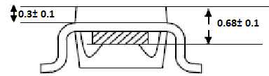
Sensor Location (Unit: mm)
Document number: DS47020 Rev. 2 - 2 21 of 23 www.diodes.com October 2025 © 2025 Copyright Diodes Incorporated. All Rights Reserved.

Please see http://www.diodes.com/package-outlines.html for the latest version.
SOT26 (Type CJ)
C1 C
Dimensions
CC1 C2 X Y C2 Value (in mm)
0.95 1.90 2.40 0.60 1.00 Y X
• • • Moisture Sensitivity: Level 1 per J-STD-020 Terminals: Finish – Matte Tin Plated Leads, Solderable per MIL-STD-202, Method 208 Weight: 0.016 grams (Approximate)
Document number: DS47020 Rev. 2 - 2 22 of 23 www.diodes.com October 2025 © 2025 Copyright Diodes Incorporated. All Rights Reserved.

IMPORTANT NOTICE 1. DIODES INCORPORATED (Diodes) AND ITS SUBSIDIARIES MAKE NO WARRANTY OF ANY KIND, EXPRESS OR IMPLIED, WITH REGARDS TO ANY INFORMATION CONTAINED IN THIS DOCUMENT, INCLUDING, BUT NOT LIMITED TO, THE IMPLIED WARRANTIES OF MERCHANTABILITY, FITNESS FOR A PARTICULAR PURPOSE OR NON-INFRINGEMENT OF THIRD PARTY INTELLECTUAL PROPERTY RIGHTS (AND THEIR EQUIVALENTS UNDER THE LAWS OF ANY JURISDICTION).
The Information contained herein is for informational purpose only and is provided only to illustrate the operation of Diodes’ products described herein and application examples. Diodes does not assume any liability arising out of the application or use of this document or any product described herein. This document is intended for skilled and technically trained engineering customers and users who design with Diodes’ products. Diodes’ products may be used to facilitate safety-related applications; however, in all instances customers and users are responsible for (a) selecting the appropriate Diodes products for their applications, (b) evaluating the suitability of Diodes’ products for their intended applications, (c) ensuring their applications, which incorporate Diodes’ products, comply the applicable legal and regulatory requirements as well as safety and functionalsafety related standards, and (d) ensuring they design with appropriate safeguards (including testing, validation, quality control techniques, redundancy, malfunction prevention, and appropriate treatment for aging degradation) to minimize the risks associated with their applications.
Diodes assumes no liability for any application-related information, support, assistance or feedback that may be provided by Diodes from time to time. Any customer or user of this document or products described herein will assume all risks and liabilities associated with such use, and will hold Diodes and all companies whose products are represented herein or on Diodes’ websites, harmless against all damages and liabilities.
Products described herein may be covered by one or more United States, international or foreign patents and pending patent applications. Product names and markings noted herein may also be covered by one or more United States, international or foreign trademarks and trademark applications. Diodes does not convey any license under any of its intellectual property rights or the rights of any third parties (including third parties whose products and services may be described in this document or on Diodes’ website) under this document.
Diodes’ products are provided subject to Diodes’ Standard Terms and Conditions of Sale (https://www.diodes.com/about/company/terms-and-conditions/terms-and-conditions-of-sales/) or other applicable terms. This document does not alter or expand the applicable warranties provided by Diodes. Diodes does not warrant or accept any liability whatsoever in respect of any products purchased through unauthorized sales channel.
Diodes’ products and technology may not be used for or incorporated into any products or systems whose manufacture, use or sale is prohibited under any applicable laws and regulations. Should customers or users use Diodes’ products in contravention of any applicable laws or regulations, or for any unintended or unauthorized application, customers and users will (a) be solely responsible for any damages, losses or penalties arising in connection therewith or as a result thereof, and (b) indemnify and hold Diodes and its representatives and agents harmless against any and all claims, damages, expenses, and attorney fees arising out of, directly or indirectly, any claim relating to any noncompliance with the applicable laws and regulations, as well as any unintended or unauthorized application.
While efforts have been made to ensure the information contained in this document is accurate, complete and current, it may contain technical inaccuracies, omissions and typographical errors. Diodes does not warrant that information contained in this document is error-free and Diodes is under no obligation to update or otherwise correct this information. Notwithstanding the foregoing, Diodes reserves the right to make modifications, enhancements, improvements, corrections or other changes without further notice to this document and any product described herein. This document is written in English but may be translated into multiple languages for reference. Only the English version of this document is the final and determinative format released by Diodes.
Any unauthorized copying, modification, distribution, transmission, display or other use of this document (or any portion hereof) is prohibited. Diodes assumes no responsibility for any losses incurred by the customers or users or any third parties arising from any such unauthorized use.
This Notice may be periodically updated with the most recent version available at https://www.diodes.com/about/company/terms-andconditions/important-notice The Diodes logo is a registered trademark of Diodes Incorporated in the United States and other countries. All other trademarks are the property of their respective owners. © 2025 Diodes Incorporated. All Rights Reserved.
Document number: DS47020 Rev. 2 - 2 23 of 23 www.diodes.com October 2025 © 2025 Copyright Diodes Incorporated. All Rights Reserved.